This thread has been locked.

If you have a related question, please click the "Ask a related question" button in the top right corner. The newly created question will be automatically linked to this question.

[FAQ] DS90UB947-Q1: MAPSEL question

Part Number: DS90UB947-Q1

Hi team

My customer Hasco is using our 947 and configure its mode_sel1, here is our question:

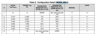
1. When our VR6=0V, the 0x4F read back value is 0x40 which means the bit[7] is 0 and that is described to be the SPWG mapping but in MAPSEL table we see it should be OLDI mapping:

2. When our VR6=0.9V, the 0x4F read back value is 0xC0 which means the bit[7] is 1 and that is described to be the OLDI mapping but in MAPSEL table we see it should be SPWG mapping.

3. Here is our 947 device marking:
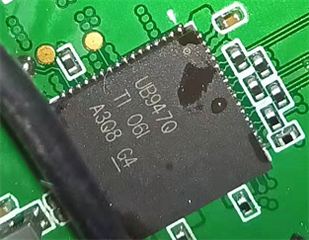
Could you please kindly help to review this phenomenon? Thank you.

  • Zirui,

    There is a typo in the datasheet and this is confusing because technically SPWG and OLDI are the same thing. In future datasheet updates we plan to clarify the naming conventions per this table:


    24 Bit Mode

    18 Bit Mode

    MAPSEL = H

    OLDI/SPWG/VESA

    4 Lane 18 Bit Mode

    MAPSEL = L

    JEIDA

    Standard 18 bit

    It is best to go by the bit position diagrams in section 7.3.4 to avoid confusion since in the industry there are many conflicts between vendors with these naming conventions anyways 

    Best Regards,

    Casey 

  • Hi Casey,

    From my customer test result, does the mode_sel1 strap correspond to the register readback value because they would like to use the SPWG, so should we need to configure MAPSEL=1? If so, should we configure mode_sel1 as #5?

  • Hello Zirui,

    Yes, for SPWG/OLDI/VESA format, use MAPSEL = H which corresponds to modes 5-8 of the table 

    Best Regards,

    Casey