This thread has been locked.

If you have a related question, please click the "Ask a related question" button in the top right corner. The newly created question will be automatically linked to this question.

DS90UB953-Q1: Abnormal operation at low temperature - 40 ℃

Part Number: DS90UB953-Q1

Hi Team,

One of our customers has the following questions:

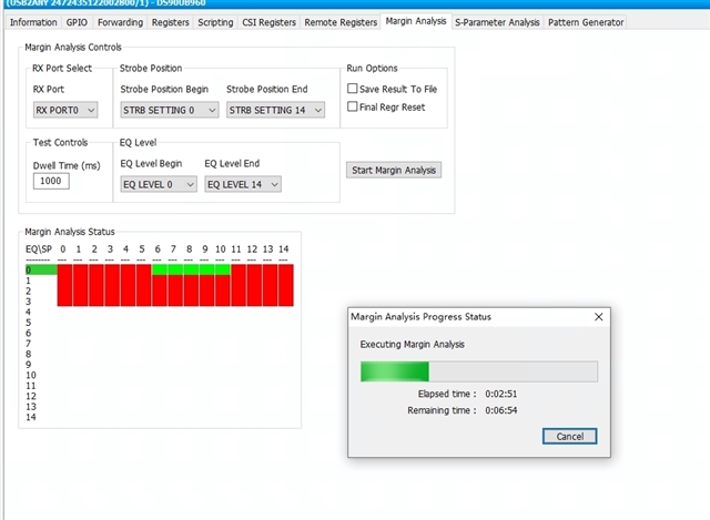
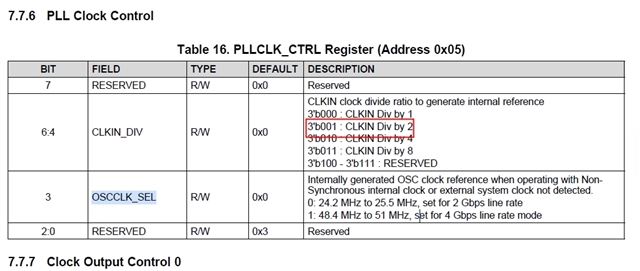
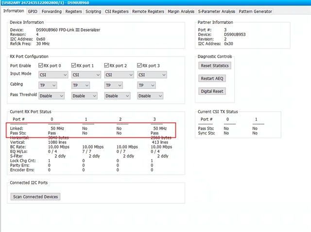
DS90UB953 is used as video output product, and 964 is used together without POC. The two SerDes are powered separately. Synchronous mode is used. CLK of 953 is provided through FPD-Link of 964.

During the low temperature (- 40) experiment, the video output is abnormal and the Link cannot be connected. Using TI's 964 demo to test FPD-Link, it is found that the Link cannot be connected at low temperature (- 40 ℃), and the link state is unstable, changing between disconnected and connected states.

At this time, the power supply of 953 is stable. Return to normal temperature and work normally. The harness and other cameras are the same set of harness, and other cameras are normal at low temperature. I don't know what may be wrong with this situation.

Best Regards,

Amy Luo

  • Hello Amy,

    The UB964 can not be used in Synchronous mode. So, If you want to pair the UB953 with this DES, you must use the UB953 in DVP mode and use an external clock source.

    If you want to use the UB953 in Synch mode, then you shall use the DES UB960 or the UB954.

  • Hi Hamzeh,

    The customer feedback:

    The DES used now is 960, synchronous mode. There is no problem at normal temperature. When it is low temperature, the linklock is disconnected and cannot be started. 

    Is the temperature protection mechanism of this register ( ALARM_SENSE_EN (Address 0x1D),T_UNDER R/W 0x0 Enable Temp Sensor under the low limit alarm) causing this problem, but we don't know how to configure these related registers to solve our current problem.

  • Hello Amy,

    are you enabling the Temp sensor alarm? If yes, which registers are you writing?

    If no, then how do you know this register is causing the problem?

    Can you send a register dump from SER and from DES in a good mode and in error mode?

  • I don't know whether this temperature protection mechanism will lead to the disconnection of Ser and des links. At the same time, I won't configure the temperature alarm mechanism. At present, the relevant registers in this part are configured by default.

    So what I want to know is whether the temperature alarm mechanism of 953 will disconnect Ser and des link? How should the temperature alarm mechanism be configured correctly? If I want to turn off this temperature alarm mechanism, how should I configure the register?

  • Hello Amy,

    the integrated in the SER is just Temp sensor, not a Temp protection mechanism. If this is correctly programmed for a certain Temp limit, it will just rise a flag once that limit is hit. The SER or DES will not do anything else. They also will not disconnect the link or lose LOCK.

  • Is it possible that the low-temperature disconnection problem is related to the change of the ripple of the 953 power supply in the low-temperature environment? Because we can't measure the ripple of the power supply in the low-temperature environment, we can only evaluate it with the normal temperature data. The ripple requirement of the 953 data sheet for the power supply is 25mV p-p. must this ripple requirement be met? If the power ripple is too large, will the link of SerDes be disconnected?

  • Hello Amy,

    you need to make sure that all specs of the Device are met all all temperatures, not only room temp.

    I have asked you in my first reply if you can send a register dump from SER and from DES in a good mode and in error mode?

  • Hi Hamzeh,

    The customer feedback:

    1. This is the register value at - 30 . At this time, the link is still linked, but if it cools down again, the link will be disconnected immediately.

    2. This is the register value of 25 ℃ at normal temperature.

    3. The link has been disconnected at - 40 , and the register value of 953 cannot be dumped.

    I read some TI materials and mentioned that power supply noise, impedance continuity of FPDLINK  line and frequency offset may affect the link stability of FPDLINK. The power supply ripple is about 20mV under normal temperature, which is already very low. Due to the limitation of the environment, we can't measure it at low temperature. Moreover, generally, the performance of this power chip will be reduced at high temperature, and the possibility that the performance will be reduced at low temperature is not mentioned.

    The routing of FPDLINK on PCB is the inner layer, with an impedance of 50 Ω. The upper and lower layers are complete strata, which should be no problem.

    Regards,

    Amy

  • Another problem with this customer:

    FDP link has an AEQ that can compensate for the change of FDP link line insertion loss. How should we configure these related registers.

  • Hello Amy,

    Can you please provide the dumps in text form, so that I can search and copy?

    Is it not possible to dump the 953 locally?

    Also,what do you have in the climate champer, the SER only or both devices?

  • Hello Hamzeh,

    The customer feedback:

    This part of the register file will be re exported in text format and uploaded.

    Our product definition is that the I2C of 953 is only pulled up, and the configuration of 953 can only be configured through 960 after 960 lock.

    There is only ser-953 in the climate chamber. Des-960 is placed outside at room temperature.

    At present, we have also done some experiments, using TI's 960 corresponding tools to test the Link margin of SER at different temperatures. The Link margin at room temperature and high temperature is very good, which is basically the best performance. When it is below - 10 ℃, the Link margin will slowly deteriorate, EQ / SP will fail, and there are more and more red branches. Wait until - 40  ℃ and the lock is completely disconnected.

    Regards,

    Amy

  • Hello Amy,

    it is clear that if the signal quality is bad then MAP results will be worst until all red.

    Please provide as I said, the dumps in text form, so that I can search and copy.

  • Hi Hamzeh,

    I'm very sorry, this customer has raised a lot of questions:

    We have tested and found that using Non-Synchronous mode is more stable at low temperature, so we have several questions about Non-Synchronous:

    1、Whether Synchronous mode and Non-Synchronous do have different requirements for peripheral circuits, especially the requirements of S11 and S12. Is Synchronous mode more stringent.

    2、Which of the two modes of Non-Synchronous external clock and Non-Synchronous internal Clock is more stable? It is better to keep the transmission stable after the change of external factors (such as S11 and S12). What is the reason?

    In addition to the difference of voltage dividing resistance on the Mode pin, whether the two Non-Synchronous modes need to change the settings of registers related to 953 and 960?

    3、What is the difference between 25M and 50M in the selection of crystal oscillator for Non-Synchronous external clock? Are the configurations different on 953 and 960?

    4、Can Non-Synchronous only run 2G? Must the AC capacitor here strictly choose 100nF + 47nF? Is the choice of AC capacitance determined by mode or rate?

    5、If we choose the Non-Synchronous mode, but we choose the combination of 33nF + 15nF for AC capacitance, is it OK? What are the risks?

    6、If our current hardware mode and software configuration work in synchronous mode, but the external clock IC input by CLKIN pin of 953 is SMD, will this affect the operation of synchronous mode

    7、 If the Mode pin of 953 is configured as Non-Synchronous external clock mode, but the configuration of 960 is Synchronous mode, can it work normally and what are the risks?

  • Hello Amy,

    1、Whether Synchronous mode and Non-Synchronous do have different requirements for peripheral circuits, especially the requirements of S11 and S12. Is Synchronous mode more stringent.

    For peripheral ckt you should modify the MODE pin resistor values and the AC-coupling caps if using 33nF.

    You need to know also that once using Non-Synch External Mode you can output CLK from SER to the Image sensor using CLKOUT pin, but if using Non-Synch with Internal CLK then CLKOUT pin is not functioning and you can't output CLK into the image sensor.

    Insertion Loss and Return Loss requirements are exactly the same. The only different is for non-Synch mode the frequency range starts a bit earlier that Synch mode due to the lower frequency back channel. So Synch BC is at 25MHz but Non-Synch BC is at 5MHz.

    2、Which of the two modes of Non-Synchronous external clock and Non-Synchronous internal Clock is more stable? It is better to keep the transmission stable after the change of external factors (such as S11 and S12). What is the reason?

    In addition to the difference of voltage dividing resistance on the Mode pin, whether the two Non-Synchronous modes need to change the settings of registers related to 953 and 960?

    We have validated all three modes thoroghly under the specified temperature range and voltage tollerences, hence all transmission Modes are stable. 

    If you change MODE pin setup then you do not need to change the registers. Only one register needs to be modified if using internal CLK which is reg 0x05[3] from default 0 to 1.

    3、What is the difference between 25M and 50M in the selection of crystal oscillator for Non-Synchronous external clock? Are the configurations different on 953 and 960?

    If you chose to use a higher frequency External CLK source (50MHz-104MHz) then you must change the Input divider from 1 to 2 as shown in the table above. This should be done in reg 0x05[6:4]

    4、Can Non-Synchronous only run 2G? Must the AC capacitor here strictly choose 100nF + 47nF? Is the choice of AC capacitance determined by mode or rate?

    Non-Synch runs at 4G or 2G.

    The AC-couplings capacitor value depends on the BC frequency. As explained in #1, the Non-Synch has lower BC frequency hence requires the 100nF + 47nF caps.

    5、If we choose the Non-Synchronous mode, but we choose the combination of 33nF + 15nF for AC capacitance, is it OK? What are the risks?

    Your BC may not work properly.

    6、If our current hardware mode and software configuration work in synchronous mode, but the external clock IC input by CLKIN pin of 953 is SMD, will this affect the operation of synchronous mode

    Sorry, I could not understand the question!

    7、 If the Mode pin of 953 is configured as Non-Synchronous external clock mode, but the configuration of 960 is Synchronous mode, can it work normally and what are the risks?

    No this is not a valid use case! Both sides must match the Mode configs.

  • Hi Hamzeh,

    Thank you very much for your reply. Another question from the customer, please help reply.

    Now it works in the Non-Synchronous   external clock(50M)  mode. When testing the link margin, it is found that the Linked here is 100MHz by default. What does the Linked frequency represent? Why does the input of 50MHz become 100MHz? At this time, when testing the link margin, the two lines will fail and the lock will be disconnected. After Digital Reset, the linked is normal.

    If CLKIN_DIV=2, the Linked clock here will become 50MHz, and the test link margin can be tested normally. What is the reason for this

  • Hello Amy,

    When testing the link margin, it is found that the Linked here is 100MHz by default. What does the Linked frequency represent? Why does the input of 50MHz become 100MHz?

    In Synchronous mode, the FPD3_PCLK is based on REFCLK input reference frequency , the FPD-Link line rate is a fixed value of 160 × REFCLK. FPD3_PCLK = 4 × REFCLK and Back channel rate = 2 × REFCLK. For example with REFCLK = 25 MHz, line rate = 4.0 Gbps, FPD3_PCLK = 100 MHz, back channel data rate = 50 Mbps.

    In Non-Synchronous mode, the Forward channel uses the external reference clock (CLKIN), and the FPD-Link line rate is typically CLKIN × 80. The Linked frequency is = 2 × CLKIN or 1 x CLKIN  depending on your divider settings. Back channel data rate is set to 10 Mbps.

    For example, with CLKIN = 50 MHz if the divider is 1, line rate = 4Gbps, FPD3_PCLK = 100 MHz, and the back channel rate is 10 Mbps, but if the divider is 2 then FPD3_PCLK = 50MHz.

    Please refer to the 953 datasheet, Table 7-6.

  • Hi Hamzeh,

    The problem we're having is that if use the 953 default FPD3_PLCK=100M, the test of the linked with TI tools is stable, but once click Linkmargin to test the Link , it disconnects. Margin couldn't test either, and the linked was OK after clicking Digital Reset again. However, with FPD3_PLCK=100M, our product works and the graphics are all fine.

    Linkmargin could be tested if FPD3_PLCK=50M and margin was good, but the FPD3_PLCK=50M did not meet our image transmission bandwidth requirements.

    So I want to know if the FPD3_PCLK=100M is something that needs to be set up to test Linkmargin properly, after all, at this time our product is working properly, and we can't just test Linkmargin.

    Our operating mode is Non-Synchronous External Clock and the external crystal is 50M.

  • Hello Amy,

    please do not relay on just doing the MAP Tool test to verify your link. This Tool result is an instant snap shot from a single system. If you want to test your system and qualify it you should use the VNA and measure the Return Loss and Insertion Loss over the complete used frequency range on different systems and make sure this fulfills our Channel specifications!