


Part Number: DP83822I
[Introduction] The difference of DataSheet's Revsion
(1) Lastest Revsion : Rev.F
English DocNo.: SNLS505F – JULY 2016 – REVISED JUNE 2021
Jananese DocNo.: JAJSEV0F – JULY 2016 – REVISED JUNE 2021
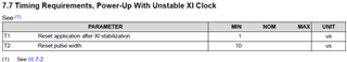
=> In chapter 7.7

(2) Old revision : Rev.E
English DocNo.: (Not downloaded)
Jananese DocNo.: JAJSEV0E –AUGUST 2016–REVISED MARCH 2019
=> No description corresponding to chapter 7-7
[Question]
What was the intention behind adding Chapter 7.7?
I guess is that it is either of the following (apologies if this is off the mark)
(1) I'm assuming a circuit that inputs a clock from an oscillator to pin XI.
If the clock is unstable immediately after power-on, the DP83822 will malfunction.
(2) There is an asynchronous reset circuit inside the DP83822, and there are provisions for reset input and clock input.
Therefore, if the sequence in chapter 7.7, Power-on - Clock input - Reset control [High ⇒ Low ⇒ High],
is not performed DP83822 does not operate normally (e.g., internal registers and buffer relationships become undefined).
At the time of circuit design circa 2021, we were designing according to Rev. E, so we did not take care of Chapter 7.7
The actual operating waveforms are described below, please let me know if there is a problem.
[Circuit & Waveforms]

- Waveforms
(1) PowerON
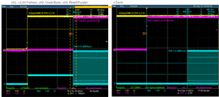
(2) Soft Reset = FPGA is reconfiged

Best regards.
