This thread has been locked.

If you have a related question, please click the "Ask a related question" button in the top right corner. The newly created question will be automatically linked to this question.

SN65HVD1782-Q1: Question about SN65HVD1782QDRQ1

Part Number: SN65HVD1782-Q1

Hello:

The customer is currently using a TI chip SN65HVD1782QDRQ1, which fails after power on. They use two chips to convert clock signal CLK and data signal SIMO of SPI signal into differential signal output. The schematic diagram is shown below. In the past year, there were 3 or 4 random failures of the chip after power on, all of which were U39 failures, which showed that the chip output level was constant.

Please ask if you have encountered similar problems, or help confirm whether there are defects in the schematic design? thank you very much!
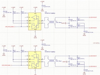
  • There is nothing strange in the schematic.

    What does "constant" mean? What are the voltages at both outputs (A and B)?

    The most common cause is overvoltage, but that does not explain why only the clock transmitter fails. Are the LED-SCLK-x signals nearer some other (high-voltage) signal? Or exposed to be touched by humans, causing ESD?

    Does U39 get hot during normal usage?

    (If the signal is unidirectional, then you do not need termination resistors at the transmitter. But this has nothing to do with this problem.)

  • Hi Jimmy,

    What is the Datarate of the application?

    Are there only 2 nodes on the differential bus - or are there more?

    For the "constant" level output: what is the output level - and is it not toggling? 

    Please let me know - as the 47pF capacitors to ground could possibly be taking too much of the impedance budget which could possibly be overstressing the driver - but with only a few failures - I want to double check the use case to see if this is the possible source of the problem.

    Best,

    Parker Dodson

  • Hi Parker & Clemens,

    1. the data rate is 500kbps;

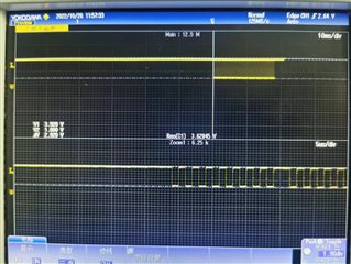
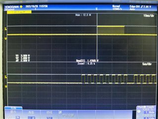
    2. for a good piece, the output is like:

    U39 OUTPUT AU39 OUTPUT B

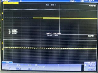
    for the failed one, the output is lke:

    failed output AA and B are the same

    3. both U39 and U40 get hot during normal usage, which has over 20℃ temp rise:the case temp can reach 47℃ in a normal ambient temparture of 25℃

    4. this is a unidirection application, U39 and U40 are only used for transfer,and there are only two nodes on the bus, both have load resistors of 120R.

    5. I tried to remove the load resistors on transmitter side, but the temp rise on U39 and U40 still the same

    6. the OUTPUT A and B is closed to 12V power supply,  but not over 70V according to the datasheet?

  • Hi Liyang,

    1. With that low of a data rate + a point to point use case I don't think the capacitors to ground should be causing any issue as the common mode impedance isn't being violated here. 

    2. Alright - both of the tests included the same input stimulus correct?

    3. Is the application usually ran in 25C conditions? Even so - a temp rise of 20C from ambient shouldn't be that much of a concern - but the temp raise may be more in higher ambient temp environments - have the fails all come from 25C testing?

    4.Alright thanks for the clarification!

    5.I don't think the load resistors are the issue - but that test pretty much confirms they aren't the problem.

    6. How close to the 12V power supply? We still only recommend -7V to 12V common mode voltage for a functional range. This device is fault protected (the 1782 is +/-30V not +/-70V like the 1781/1780) so I don't expect damage - but it could cause some strange behavior if outside rec. operating range. Can the test with a failed unit be done where there isn't a common mode voltage applied - if the same problem is occurring that may indicate damage but I want to be able to cross off as many variables as possible to see what the origin of the issue possible is. 

    7. Are there any transient pulses that could have occurred in the system either on VCC or the A/B pins during testing that you are aware of? 

    Please let me know!

    Best,

    Parker Dodson 

  • Hi Parker,

    1.yes, the test is taken with the same input singals, there is slightly voltage ripple when input pin has stimulus, but never rise up.

    2. the failure ones are all found in 25C condition, while good ones can be safely used in 85C ambient temparture, I agree the temp rise is not a concern

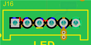
    3. this is the pcb layout for the output of U39 and U40, you can see the 12V layer is surrounding the output pins of U39 & U40, the clearance is 0.254mm, but I dont think it chould damage the chip.

    4. the SGND is connnected to the other node, and is not a isolated applicaiton, so I think there may be not a common mode voltage  whould be applied on the chip

    5. you remind me that the output of these chips dont have a tvs diode or any esd protect parts, is it possible broken by human touch? since the SGND is floated one?

  • one more thing:

     the waveform in oscilloscope  is taken in single board test, while the output is not connected to the other node. so I think it is broken, not a fault protect behaivor.

  • Hi Liyang,

    Thanks for the additional information!

    When you say the SGND is a floated one - is this connected to return termination of the 5V-PFC source and just not connected to an Earth Ground? I am a bit confused what you mean by saying the SGND is floated - I apologize.

    This part is ESD rated:

    So while ESD damage is possible - the HBM is +/-16kV - so there is ESD protection up to the above levels. 

    That being said - if there is a transient or surge event - this device does not have integrated TVS diodes and isn't surge rated. 

    Please let me know on the SGND - after that it may be necessary to look into our return process for the failed units.

    Best,

    Parker Dodson

  • Hi Parker,

            Sorry for not accurately explaining about the SGND.

            In our Appilcation, the controller board share the same SGND for MCU and voltage sampling circuits of Grid, which is not Isolated, so the SGND could not be directly connected to CHASSIS, for now the SGND is connected to CHASSIS through a 1nF Y cap. 

            Both nodes are reference to SGND,  5V-PFC & 12V-AUX are all return to SGND. 

            I will take a look at power-on, power off , human touch and do dielectric strength test for the whole system to see if any transient surge occur on output pins of chips. 


  • Hi Liyang,

    No problem! Thanks for explaining - its clear now. So that should be fine it doesn't require a direct CHASSIS connection - so using a Y cap as the connection point is fine.

    Please let me know what the results of your testing is so I can see what other support I can offer.

    Best,

    Parker Dodson