


Good morning,
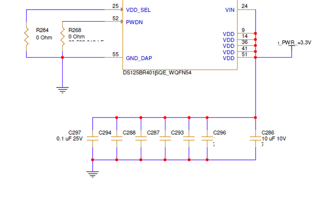
I was reviewing and old design and found out that the power design is quite wrong. As you can see with the provided screenshot, VDD_SEL is tied to GND. According to the datasheet, tying this pin ground enables the internal LDO which provides a regulated output of 2.5V. Also according to the datasheet, if I provide a 3.3V power rail to the IC and enable the internal LDO through VDD_SEL, the VDD pins should be routed individually with a local bypass capacitor of 0.1uF... But, as you can see in the provided screenshot, the +3.3V power rail is also tied to the VDD pins while the internal LDO is enabled. Surprisingly, it doesn't seem to have much impact on the IC... After the validating with the absolute maximum rating of the VDD pin (2.75V), I'm wondering why the die didn't fry or had any impact on the IC.
Am I missing something about this particular power topology? What impact am I suppose to expect from the mentioned design mistake?
Kind Regards
