A related question is a question created from another question. When the related question is created, it will be automatically linked to the original question.
If you have a related question, please click the "Ask a related question" button in the top right corner. The newly created question will be automatically linked to this question.
Currently we don't have a model of this device (and its not currently in our backlog) - and our templates for simple models do not capture the auto-direction feature of this device (which I am guessing customer is interested about - so we don't have great alternative models either).
Is there any specific question on operation and performance about the device? Most RS-485 systems are pretty linear so we usually can extrapolate a decent amount of information without a model, but understanding what you are trying to do with the model would be helpful to see what support I can provide at this time.
Thanks for your answer and as a conseguence to the model unavaliability I need to ask some question to fully understand the behaviour of THVD1406 and find its best usage for tha functions of my card.
1) On the datasheet REVISED Novmber 2021 Paragraph 8.4 Device Functional Model I read "When SHDNbar is Low both the Drive and the Receiver are turned OFF and the device is in shutdown Mode". That means I have to keep the SHDNbar pin driven HIGH or Open (due to internal PullUp) until if I want to keep the device functional?
In other words when SHDNbar is low no driving no receiving functionality as stated in Table 8.1 Drievr Function Table.
2) If what stated at point 1) is correct in the Table 8-2 Receiver Function Table the SHDNbar Pin is assumed to be HIGH for all the row reported in the Table (there is no column that specify the status of SHDNbar for veery Row)
1. You are correct - when /SHDN is low the device will be in shutdown mode and drivers and receivers are off - as explained right above table 8.1 in datasheet.
2. It seems that table 8.2 is assuming /SHDN is always open or high (device not in shutdown) for the receiver table. There is two reasons that this assumption should be valid:
2.A) Direct Quote Highlighted from section 8.4
2b) Auto-direction is implied in 8-2 (highlighted section below) and auto-direction requires /SHDN and /RE to be held high or left floating - so the /SHDN being high/open is implied
Ultimately this device should be used where /SHDN and /RE are held high (auto-direction mode) - if you don't need this feature than the THVD1400 is essentially the same device without auto-direction and /RE controls receiver and instead of /SHDN its DE which only controls the driver - so it is a bit simpler to use.
But in general - there is an assumption that /SHDN is open/high based for table 8.2 - but it isn't explicitly stated in table (its explicitly stated in the paragraph above table 8.1)
Please let me know if you have any other questions!
Unfortunately we have problem to get the THVD1406 working as we expected acoordingly with you confirmed in previous answer. Let me insert the Testbench and below the details of the circuit
and details of TX and RX circuitry
We tried two different way of operation:
First Mode of operation
0) We are driving data on the TX pin D accordingly with an RS232 protocol at 115.2 Kbit/sec.
1) We TOOK OUT the two resistance between REbar and SHDNbar on both TX and RX transceiver (REbar and SHDNbar on both TX and RX transceiver Not Shorted). We pulled the SHDNbar of both TX and RX transceivers High by resistors. We drived the REbar of the TX High by the uP and the REbar of the RX transceiver Low. The D pin of the RX transceiver is drived High by the uP. The D pin of the TX transceiver is drived by the uP.
Result: No data present on R pin of RX transceiver (we have a steady level) NOK
Second Mode of operation
0) As above
1) We shorted by a 0 Ohm resistor the REbar and SHDNbar on both TX and RX transceiver. We pulled down the REbar by resistor on RX trasceiver. We drived the REbar of the TX transceiver High by the uP. The SHDNbar pin on both the TX and RX transceiver are left Open.
Result: All is working OK.
I hope that my description could be clear. Please let me know if not.
Could you have any suggestion about such behaviour?
First - this device is not an RS-232 device -and doesn't conform to the RS-232 standard (it conforms to the RS-485 standard) - so while I don't think the single ended signal interface is really that problematic the PHY layer does not comply with RS-232; this doesn't mean it will necessary fail - but it won't be able to withstand all RS-232 inputs (from other devices) or be rated to the same levels as RS-232.
That being said:
So here is a more clear function table.
Situation 1 as you describe - I have a few questions:
1. On the TX Device A/B pins have you confirmed the output differential voltage?
I ask as you are toggling the "D" input on the RX transceiver - and how you have it wired the RX transceiver is going to be outputting - it seems like you could have data collision on the
Situation 2 as you describe:
TX is auto-direction mode and RX is in RX mode - always listening; which makes sense why it is working in that situation.
Situation 2 is a valid approach to this design - but situation one seems like there could be data collisions that cause no data to be received at the RX devices "R" pin.
Please let me know if I have misunderstood any of your tests.
The attached Truth table is absolutely Clear. (Just a curiosity: what mean the star near OFF on the third Row TX Status Column?)
Let me clarify a little bit:
0) You are right it's not an RS232 standard protocol. What I ment is that on the TX transceiver pin D with no info to send I have a logic high level. The payload is a character wrapped in a low level start bit and an high level stop bit. But I suppouse (please confirm me if I am right) that using the correct logic level on the input pins the transceiver should work regardless the pattern asserted.
Situation 2
As REbar and SHDNbar are shorted on the RX transceiver. When we pull down the REbar on RX trasceiver the SHDNbar is pulled down as well. Accordingly with truth table I cannot receive data on the R pin of the RX transceiver as the RX Status is OFF.
Situation 1
You are absolutely right as there is something weird on both the differential lines during transmission that could be related to a sort of collision. But how can I have a collision with pin D high and REbar pin low on the RX transceiver as in your table the TX Status should be OFF (I have only one TX transceiver and one RX transceiver on the line).
Could you please scketch what has to be the correct waveform on pins A and B during a transmission related to the logical level on pin D of the TX transceiver.
We are in a big trouble as we cannot use the THVD1400 (we don't need the autodirection mode) as we bought 5000 pieceis of THVD1406.
The star means that TX stays on for a short time after D goes high.
The THVD14x6 is designed for UART protocols with a start bit and idle high, otherwise, the auto-direction control would not work. When D goes from low to high, the transmitter actively drives high, then waits for a time specified by tauto-dir before it goes idle:
If the data ends with 1 bits, then it is possible that the line goes idle before all of the data has been transmitted. For example, this happens when the data byte is 11001111:
This is not actually a problem. When the line is idle, the termination resistor will force the differential voltage to zero, which is recognized by the receiver as high. (Some buses also have fail-safe pull-up/-down resistors to ensure that idle A/B lines are high/low.)
At 115.2 kbaud, the length of a single bit is 8.7 µs. So in this case, the typical tauto-dir is shorter than a bit.
What do you mean with "weird"? Please show an oscilloscope trace of the A/B lines. (If possible, tell the oscilloscope to compute A−B.)
Thanks for your answer. Tomorrow I will send you the oscilloscope trace of the A-B lines when the transmission is NOT OK in our test conditions.
Let me ask you a couple of question:
1) What are the logic levels on REbar and SHDNbar pin respectively on the TX transceiver and the RX transceiver related to the waveform you reported above?
2) Do you confirm me that when the SHDNbar pin is LOW regardless of logic levels on REbar and D pins both the trasmitting and the receiving functionality are disabled and in such situation (trasceiver disabled) what is the logic level on the R pin?
1) Both are high (this is the auto-direction mode). You would pull /SHDN low when you wanted to shut off the transceiver for power saving. You would pull /RE low when you wanted to always receive data, even when you're currently sending.
2) Yes. /SHDN overrides all other signals. In that case, R is floating, so if you ever use the shutdown mode with a powered-on microcontroller, you should use a pull-up resistor.
3) There is the RS485-HF-DPLX-EVM; it's just a breakout board.
I agree with Clemens' response. Please let me know if you have further questions. We are looking forward to the oscilloscope capture that will be provided. Parker is currently out of office, so I will do my best to assist this inquiry.
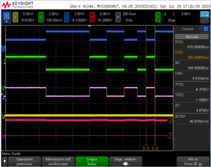
Below you can find some oscilloscope capture relating to a test setup consisting in a couple of transceiver called repectively TX and RX tha share the same couple of lines.
Description of waveform:
CH1 -> RE_TX (pin #2 of TX transceiver) YELLOW
CH2 -> Linea A (connector X2, pin #1) BLUE
CH3 -> Linea B (connector X2, pin #2) GREEN
CH4 -> D_RX (pin #4 of RX transceiver) RED
M1(A-B) -> CH2-CH3 -> Linea A-B PINK
The MicroProcessor is driving HIGH the RE_TX pin that has a pulldown resistor of 10K.
The MicroProcessor is driving LOW the RE_RX pin that has a pulldown resistor of 10K.
At this point we isolated (OPEN) both the REbar and the SHDNbar pin on the TX transceiver and the RX transceiver and the BLUE, GREEN and PINK traces do not change.
Let me remember that the speed is of 9600Bit/sec.
The only way to get a correct behaviour is to control such THVD1406 devices as if they were a THVD1400. We doublechecked the device name on the package.
We are fully confused as we have 5000 devices but not idea on how to let them work.
One more interesting info "taken on the buzzer": if we take out the RX transceiver from the line (I have only the TX on the line the behaviour seems to be correct ... the RX is forcing an HIGH despite the RE LOW and the D HIGH) as in the picture below (do not consider the YELLOW and RED traces). I said seems as with a bit time around 100us I don't see for the Ones Bit the discharge of the lines after 8usec having two 120Ohm resistor as termination at the end of the lines ... but as already stated I am totally confused.
The captures show that the transmitter works correctly.
The receiver does not output anything. I suspect this is because its /SHDN is low. (I do not care what the resistors or microcontroller are doing; please measure the voltage at the pin.)
The differential bus voltage should go to zero, if there are termination resistor. What resistance do you measure between A and B?
Below you can find some oscilloscope capture relating to a test setup consisting in a couple of transceiver called repectively TX and RX tha share the same couple of lines.
Description of waveform:
CH1 -> RE_RX (pin #2 di U14) YELLOW
CH2 -> Linea A (connettor X2, pin #1) GREEN
CH3 -> Linea B (connettor X2, pin #2) BLUE
CH4 -> SHTDN_RX (pin #3 di U14) RED
M1(A-B) -> CH2-CH3 -> Line A-B PINK
The impedance seen between line A and line B is about 60 Ohms (2 120 Ohms in parallel)
The only way we empirically found to let it work is controlling both the transceivers as they were THVD1400 chips (using the /SHDN pin as it was the DE pin).
It seems that the receiver (despite the /RE is low) is transmitting an High. If I disconnect the receiver the waveform on line A and B are OK. The receiver as you stated is not working. With 60 Ohms of impedance between line A and line B I should expect a line discharge starting after 8usec. I don't see such discharge even when the receiver is disconnected therefore it seems that even the TX transceiver is not working properly.
Thanks again for your patience and have a nice weekend
Are you able to get a scope shot with the following signals:
CH1 = R (pin 1)
CH2 = A (pin 6)
CH3 = B (pin 7)
CH4 = D (pin 4)
When:
/RE (pin 2) = LOW
/SHDN (pin 3) = HIGH or float
Input a square wave on the drive data input "D" pin 4, then we should see that the RS-485 signals are outputting correctly, as well as the signal reflected back on RXD (pin 1). I just want to see if the device can pass a simple loop back test.
Would you be able to take pictures of the top-side marking of each device under examination?
Have you tried an A-B-A swap? Find the faulty unit, replace with a known good unit, and then try the faulty unit again to see if the error tracks with a particular device? Or you might find that both devices do not function properly.
I got what is written on top side of the two devices (TX and RX) under examination:
First Row: 1406
Second Row: [Logo TI] 23T
Third Row: A8KT G4(underlined)
Tomorrow I will provide you
1) The waveform of loopback with the TX ONLY. Is it correct?
2) Swap the connection A-B from TX to RX transceiver (normally I should get an inversion). Is it correct?
Note: We have 5000 devices of the same Lot as specified above. We tested 10 devices getting the same bad result. We get always good result with all 10 devices if we control them as THVD1400.
I am having a difficult time looking up this specific device in our system. I can't seem to trace it back to one of fab sites. Do you have the top-side markings of a good device and another bad device?
1) The waveform of loopback with the TX ONLY. Is it correct?
If you have access to a 4-channel scope, I was wanting to look at the logic input on "D", the RS-485 bus (A & B pins), and "R" pin. The input of the RS-485 bus signals is the output of the driver.
2) Swap the connection A-B from TX to RX transceiver (normally I should get an inversion). Is it correct?
Sorry I should have been more specific here.
The A-B-A swap I am talking about is about device "A" (known bad device), "B" (known good device). The idea is to start with a known device that fails in the system, switch it out for a working device, and then re-test with the bad device to see if the failure follows a particular device. IF the system only fails when device "A" is in the circuit, then you know that there is something off with the bad device. If you can't trace the failure, and the failure persists across both "A" and "B" devices, then the problem is more likely a system error, implementation error / incorrect usage of the part. But since there are devices of the same part number that are both failing and working, it makes sense to check both a bad unit and good unit on the same design to see if the failure tracks.
It is possible during manufacturing that the 10 bad devices that were counted could have been caused by EOS or ESD events during the manufacturing of the product. Moving parts in assembly may cause high amounts of static electricity that could potentially damage a device.
Just to double check on my end, there are some THVD1406 devices that work correct?
We are waiting for devices from a different reseller for the end of the week to work with them hoping they belong to a different Lot. I will provide the Lot data and the waveform for this devices.
We tested three different devices combining them and swapping between TX and RX position. The result are consistent. They works only if we control them as they were THVD1400 devices. If we control them accordingly with THVD1406 behaviour none of them is working properly both in TX and in RX. They don't work in TX regardless with or without the RX. If I test a TX without the RX the waveform A and B seems correct because there is not a conflict (both transceiver driving the lines) on the lines but the discharge of the lines is missing (feature specific of THVD1408 device).
I will do the test of point 1) above togheter with all regression test on the coming devices.
Please let us know when you get the other lot information - as what Tyler pointed out could be very problematic as that could indicate the part is counterfeit - and for that lot if its not in our system I would ask that you please go to our anti-counterfeit page here https://www.ti.com/support-quality/quality-policies-procedures/anti-counterfeit.html.