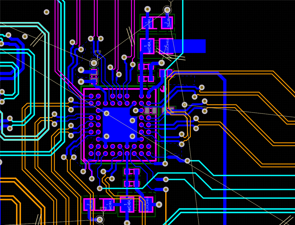
Hi everyone,
My design at present time involves smallest tracks on bottom layer (blue) with a width of 83 um.
Is there way to make these tracks larger? 90 um or even 100 um?
Thanks.
This thread has been locked.
If you have a related question, please click the "Ask a related question" button in the top right corner. The newly created question will be automatically linked to this question.
Hi everyone,
My design at present time involves smallest tracks on bottom layer (blue) with a width of 83 um.
Is there way to make these tracks larger? 90 um or even 100 um?
Thanks.
Hi,
Please see this app note, https://www.ti.com/lit/an/spraa99c/spraa99c.pdf, in particular section 2. Can you use micro blind via option to create escape option from the BGA?
Thanks
David
Hi,
I made a design with 3615 vias and the manufacturers told it is very difficult to make.
So for the HD3SSXXX I decided to use tracks with a width of 90um.
Hi,
Are you ok with the width of 90um or looking for more support?
Thanks
David
Hi,
Are you looking for a wider than 90um trace, or are you ok with the 90um trace?
Thanks
David
It would be wonderful if we could have 100 um but with a space of 250 um between balls, I don't see the solution.
In fact there are 2 options:
1/ a track with a width of 83.3 um and a space of 83.3 um
2/ a track with a width of 90.0 um with a space of 80.0 um
The option selected is not the same for several manufacturers.
Hi,
Looking at our HD3SS215EVM, the EVM is using 83um wide trace.
Thanks
David
Hi David,
Thanks for reply.
What is cheaper, 83.3/83.3 or 90/80?
Good question.
Michel
Michael
I honestly don't know, you may want to check with the PCB vendor on the cost difference between the two.
Thanks
David
I would suggest it is better to have a larger track.
I asked the question "what is the best option?", I never got the same answer...
Michael
The critical trace of HD3SS215 is the high speed differential trace. The differential trace needs to be controlled impedance traces which is calculated based on the trace widths for the board materials and adjacent ground or power planes in the layer stackup of the board. So I would go with the width that would result in controlled impedance match with your targeted impedance as close as possible.
Thanks
David
I agree with you, David. This is 90 um which is the nearest from the target.
Now the tracks with 90 um are short compared to the overall length.
Hi,
I don't see an issue with it. You want to keep it as short as possible to minimize the impedance mismatch as much as possible.
Thanks
David