This thread has been locked.
If you have a related question, please click the "Ask a related question" button in the top right corner. The newly created question will be automatically linked to this question.
Hello everyone
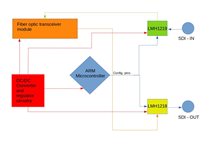
I'm develop a fiber optical to SDI bi-directional converter using LMH1219 as TX and LMH1218 as RX.
I wrote the code following the Programming Guide the both devices but the LMH1218 don't show the image that LMH1219 is received.
I would like to know if I can send the code snippet relating to the device settings so that you can analyze it and if there is an error you can help me correct it.
Can I to send?
Thanks
Marcelo
Alphacine
Hi Marcelo,
Sure you can send this code snippet. Please include a block diagram as well.
Regards, Nasser
Hi Nasser,
Thank you for receive my inquire, above my code and block diagram.
Code:
void Config_Chip_TX()//Rotina de configuração do chip conversor de fibra para SDI como TX { //Para operacao de escrita devemos colocar 0 antes do endereco //Para operacao de leitura devemos colocar 1 antes do endereco //---------Configuracoes------------------------------------------------ /*habilita a pagina do registrador CTLE/CDR HAL_GPIO_WritePin(GPIOA, CS_1_Pin, 0); operacao_tx = 0x00; endereco_tx = 0xFF; dado_tx = 0x04; mascara_tx = 0x07; comando_tx = operacao_tx+endereco_tx+dado_tx+mascara_tx; HAL_SPI_Transmit(&hspi1, &comando_tx, 1, 100); HAL_GPIO_WritePin(GPIOA, CS_1_Pin, 1); HAL_Delay(100);*/ //habilita a pagina do registrador CableEQ/Drivers HAL_GPIO_WritePin(GPIOA, CS_1_Pin, 0); operacao_tx = 0x00; endereco_tx = 0xFF; dado_tx = 0x05; mascara_tx = 0x07; comando_tx = operacao_tx+endereco_tx+dado_tx+mascara_tx; HAL_SPI_Transmit(&hspi1, &comando_tx, 1, 100); HAL_GPIO_WritePin(GPIOA, CS_1_Pin, 1); HAL_Delay(100); //habilita IN0 para OUT0 HAL_GPIO_WritePin(GPIOA, CS_1_Pin, 0); operacao_tx = 0x00; endereco_tx = 0x31; dado_tx = 0x20; mascara_tx = 0x30; comando_tx = operacao_tx+endereco_tx+dado_tx+mascara_tx; HAL_SPI_Transmit(&hspi1, &comando_tx, 1, 100); HAL_GPIO_WritePin(GPIOA, CS_1_Pin, 1); HAL_Delay(100); //habilita a pagina do registrador CableEQ/Drivers HAL_GPIO_WritePin(GPIOA, CS_1_Pin, 0); operacao_tx = 0x00; endereco_tx = 0xFF; dado_tx = 0x05; mascara_tx = 0x07; comando_tx = operacao_tx+endereco_tx+dado_tx+mascara_tx; HAL_SPI_Transmit(&hspi1, &comando_tx, 1, 100); HAL_GPIO_WritePin(GPIOA, CS_1_Pin, 1); HAL_Delay(100); //habilita controle independente das saidas OUT0 e OUT1 HAL_GPIO_WritePin(GPIOA, CS_1_Pin, 0); operacao_tx = 0x00; endereco_tx = 0x09; dado_tx = 0x20; mascara_tx = 0x20; comando_tx = operacao_tx+endereco_tx+dado_tx+mascara_tx; HAL_SPI_Transmit(&hspi1, &comando_tx, 1, 100); HAL_GPIO_WritePin(GPIOA, CS_1_Pin, 1); HAL_Delay(100); //habilita a pagina do registrador CableEQ/Drivers HAL_GPIO_WritePin(GPIOA, CS_1_Pin, 0); operacao_tx = 0x00; endereco_tx = 0xFF; dado_tx = 0x05; mascara_tx = 0x07; comando_tx = operacao_tx+endereco_tx+dado_tx+mascara_tx; HAL_SPI_Transmit(&hspi1, &comando_tx, 1, 100); HAL_GPIO_WritePin(GPIOA, CS_1_Pin, 1); HAL_Delay(100); //habilita reclocker HAL_GPIO_WritePin(GPIOA, CS_1_Pin, 0); operacao_tx = 0x00; endereco_tx = 0x1C; dado_tx = 0x80; mascara_tx = 0xE0; comando_tx = operacao_tx+endereco_tx+dado_tx+mascara_tx; HAL_SPI_Transmit(&hspi1, &comando_tx, 1, 100); HAL_GPIO_WritePin(GPIOA, CS_1_Pin, 1); HAL_Delay(100); } void Config_Chip_RX() { //Para operacao de escrita devemos colocar 0 antes do endereco //Para operacao de leitura devemos colocar 1 antes do endereco //---------Configura para modo CD------------------------------------------------ //acesso ao regustrador da pagina compartilhada HAL_GPIO_WritePin(GPIOA, CS_2_Pin, 0); operacao_rx = 0x00; endereco_rx = 0xFF; dado_rx = 0x04; mascara_rx = 0x07; comando_rx = operacao_rx+endereco_rx+dado_rx+mascara_rx; HAL_SPI_Transmit(&hspi1, &comando_rx, 1, 100); HAL_GPIO_WritePin(GPIOA, CS_2_Pin, 1); HAL_Delay(100); //seleciona IN0 para OUT0 HAL_GPIO_WritePin(GPIOA, CS_2_Pin, 0); operacao_rx = 0x00; endereco_rx = 0x31; dado_rx = 0x01; mascara_rx = 0x03; comando_rx = operacao_rx+endereco_rx+dado_rx+mascara_rx; HAL_SPI_Transmit(&hspi1, &comando_rx, 1, 100); HAL_GPIO_WritePin(GPIOA, CS_2_Pin, 1); HAL_Delay(100); //acesso ao regustrador da pagina compartilhada HAL_GPIO_WritePin(GPIOA, CS_2_Pin, 0); operacao_rx = 0x00; endereco_rx = 0xFF; dado_rx = 0x04; mascara_rx = 0x07; comando_rx = operacao_rx+endereco_rx+dado_rx+mascara_rx; HAL_SPI_Transmit(&hspi1, &comando_rx, 1, 100); HAL_GPIO_WritePin(GPIOA, CS_2_Pin, 1); HAL_Delay(100); //detecção de operação normal em IN0 HAL_GPIO_WritePin(GPIOA, CS_2_Pin, 0); operacao_rx = 0x00; endereco_rx = 0x14; dado_rx = 0x00; mascara_rx = 0xC0; comando_rx = operacao_rx+endereco_rx+dado_rx+mascara_rx; HAL_SPI_Transmit(&hspi1, &comando_rx, 1, 100); HAL_GPIO_WritePin(GPIOA, CS_2_Pin, 1); HAL_Delay(100); //acesso ao regustrador da pagina compartilhada HAL_GPIO_WritePin(GPIOA, CS_2_Pin, 0); operacao_rx = 0x00; endereco_rx = 0xFF; dado_rx = 0x04; mascara_rx = 0x07; comando_rx = operacao_rx+endereco_rx+dado_rx+mascara_rx; HAL_SPI_Transmit(&hspi1, &comando_rx, 1, 100); HAL_GPIO_WritePin(GPIOA, CS_2_Pin, 1); HAL_Delay(100); //OUT0 reclocked HAL_GPIO_WritePin(GPIOA, CS_2_Pin, 0); operacao_rx = 0x00; endereco_rx = 0x1C; dado_rx = 0x08; mascara_rx = 0x0C; comando_rx = operacao_rx+endereco_rx+dado_rx+mascara_rx; HAL_SPI_Transmit(&hspi1, &comando_rx, 1, 100); HAL_GPIO_WritePin(GPIOA, CS_2_Pin, 1); HAL_Delay(100); }
Regards, Marcelo
Hi Marcelo,
A). Please allow me to make sure i understand this block diagram. LMH1219 has two 100-ohm high speed outputs. Why didn't we use one of these outputs and provide to LMH1218 100-ohm high speed inputs? Or perhaps LMH1218 high speed input is coming from the optical module receiver?
B). Does LMH1219 shows lock indication? Registers above does not seem to show this?
C)> The same for LMH1218. Please review LMH1218 programming guide and let us know cdr.0x03 content.
D). Is it possible for you to use LMH1219 GUI? You can do this as long as you are using SMBus interface. GUI sets up the device as required. Also, GUI top level provides us with status of both LMH1219 and LMH1218 devices.
Regards, Nasser
Hi Nasser,
I will try to answer your questions...
A) The LMH1219 will receive the SDI signal send by an camera, for example, and delivered to a fiber optic transceiver to this send to another equipment video. However, the LMH1218 will be receive another signal by fiber optic transceiver provenience another equipment video and will delivery to the SDI Out to 3th equipment video work with this signal. Note that is the different signals to different pourposes.
B) Yes, the LMH1219 shows lock indication when it has a signal in the input pins.
C) The LMH1218 maintain the lock indication full time, independently if has or no signal to delivery.
D)No, unfortunately no because I'm to use the prototype board to develop the firmware to configure this devices and change the communication method will cause the loss this boards and I will need to redraw the all project and I spandex more time with this project.
Regards, Marcelo
Hi Marcelo,
Hope you're doing well, I'm going to assist with Nasser.
C) The LMH1218 maintain the lock indication full time, independently if has or no signal to delivery.
Note that is the different signals to different pourposes.
B) Yes, the LMH1219 shows lock indication when it has a signal in the input pins.
For further help in debugging the code please refer to this video on SPI: https://training.ti.com/spi-access-using-fpga-or-asic-using-lmh12xx-12g-sdi-devices
Best,
Nick