A related question is a question created from another question. When the related question is created, it will be automatically linked to the original question.
If you have a related question, please click the "Ask a related question" button in the top right corner. The newly created question will be automatically linked to this question.
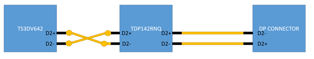
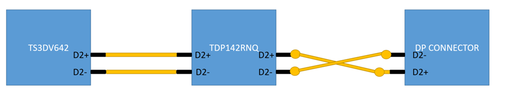
Are you asking which of the two block diagrams you have provided is more desirable?
If so, the signals crossing should take place where the signal traces are the shortest, and where you can have the crossover be perpendicular to each trace. I can't tell which one fits that criteria based off of the block diagram. It is also important to note that the TDP142 only has input equalization, so there will be more flexibility at that end.
The via will add some signal degradation that will need to be compensated for. Therefore, if you implement a via before the TDP142 input then the TDP142 may be able to help equalize the effects of the added via depending on the total amount of signal attenuation you already have at the pre-channel of the TDP142. If the via is placed at the post-channel then the devices downstream to the DP connector will have to be able to handle the losses associated with the additional via.