This thread has been locked.

If you have a related question, please click the "Ask a related question" button in the top right corner. The newly created question will be automatically linked to this question.

SN65C1168E: SN65C1168ENSR replacement

Part Number: SN65C1168E
Other Parts Discussed in Thread: AM26LV32E, AM26LV31E, THVD1424, THVD1451, THVD1452,

hi,

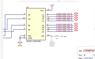
my previous designer created a project and placed a SN65C1168ENSR from rs422 conversion, but it is a 4.5 - 5vdc supply only, please correct me if i am wrong.

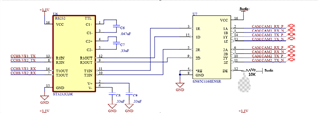
i don't have any 5vdc on my board, so i want to use a 3.3vdc support  RS422 converter, i am looking for the recommendations.

  • Hi Mohammad,

    So all of our dual channel RS-485/RS-422 transceivers are 5V only. 

    That being said - there are 2 pathways forward - but they all require multi-chip solutions. 

    Generalized Option 1: Use Quad 3.3V  RS-422 devices. 

    The AM26LV31E is a quad 3.3V RS-422 driver and the AM26LV32E is a quad 3.3V RS-422 receiver. 

    The trade off for using this device is that it looks as if the one node you have shown above both acts as a transceiver - i.e. the same node is sending and receiving information. If communication must be bidirectional than every node will need an AM26LV32E to receive a signal and the every node will also need an AM26LV31E to act as a driver. Since you have only used  two channels the two unused channels of the AM26LV3xE devices will take up board space. 

    Generalized Option 2: Use 2 single channel Full-duplex RS-485/RS-422 devices. 

    So we don't really focus on pure RS-422 anymore - but our RS-485 devices are electrically compliant with RS-422 standard (RS-422 standard can be thought of as a subpar version of RS-485 because that is basically what it is)  - so if you choose a full-duplex RS-485 device it will be able to work as an RS-422 device no issue (RS-422 is always multi-drop which for bi-directional communication would require at least two differential buses - RS-485 is multi-point so can have bi-directional communication on 1 differential pair) 

    With that being said some devices that may interest you and should be able to handle your application okay are the following options:

    1. THVD1424 - this is our Flexible RS-485 transceiver. It can be operated from a single 3.3V supply, work as a half or full-duplex device (default is full-duplex), it has an integrated termination resistor that is switchable, can communicate up to 20Mbps by default but if you switch on slew rate limiting the device will max out at 500kbps (in case you are working with slower data streams the slew rate limiting can help mitigate some emissions issues). It also does allow for separate logic supplies - which may not be necessary for your current application - but it is a possible option.  This device may add some features that you don't need - but its flexibility allows it to be placed in a wide array of varied applications and might prove interesting to you. 

    2. THVD1451 or THVD1452. These are full-duplex RS-485 transceivers that can communicate up to 50Mbps and from a use case perspective are very similar to initial device. They operate from 3V to 5.5V on VCC (best performance is when VCC =5V - but that will be the same for all RS-485/RS-422 devices where there is an option of 3.3V or 5V). The difference between THVD1451 and THVD1452 is that the THVD1451 the receivers and drivers are always active and the THVD1452 has external enables that can enable disable the receiver or driver. 

    Essentially if you go with generalized option 2 the tradeoff between THVD1424 and THVD1451/2 is that the THVD1424 is a bit overkill for what you need in terms of features but its max default speed is up to 20Mbps which will cover the entire RS-422 operational speed range (usually up to 10Mbps) without going too much over and has the ability to limit its slew rate for data rates <= 500kbps compared to the THVD1451/THVD1452 which has a max speed of 50Mbps - which means it will have a much faster slew rate regardless of actual data rate used - which may increase emission generation on the bus as well as make layout much more important. 

    CONCLUSION

    There are a few work-arounds but they will increase the number of IC's you will need. To save the most space on the PCB and generally for better performance (our RS-422 devices are also much older than our current THVD devices for RS-485/RS-422 applications) I would opt for generalized option 2 that uses Full duplex RS-485 devices (which can cover RS-422 without issue) as you will probably have better performance and use far less board space. 

    Please let me know if you have any other questions and I will see what I can do!

    Best,

    Parker Dodson

  • Hi parker,

    thank you for the replay, i understand it, i will change the device to a single channel which has a 3.3vdc option.

    but for this board i decide to use an external 5vdc the circuit is below

    i see the signal on the pin 15, its a 3.3v TTL but on the pin 14 and 13 are just high, i am i missing something in the circuit?

  • Hi Mohammad,

    No major issue with the proposed solution that you have. 

    The ST RS-232 device has a VOH(min) of VCC - 0.6V, but typically VCC - 0.1V for 1mA of current - since the SN651168E has VIH(min) of 2V and VIL(max) of 0.8V - the 3.3V device should be able to control the Sn65C1168E without issue - so that would be the R1OUT and R2OUT of the RS-232 device going into the 1D and 2D input pins.  It is a decent idea to have some sort of pull-up or pull-down on these lines so that you have default logic levels and your outputs don't glitch.  SN651168E is TTL and LVTTL input compliant - but its single ended outputs I believe are standard TTL. The differential pins are not TTL level - they are RS-422 levels - so differential output  (between Y and  Z) is minimum of 2V across 100 ohms and the receiver thresholds are >=200mV and  <=-200mV for the VIT+ and VIT- thresholds respectively (RS-422/RS-485 standard values) 

     It looks as if the ST3232C T1IN and T2IN pins have a max voltage rating independent of device VCC - so it looks like the T1IN and T2IN pins are 5V tolerant and should be able to handle the outputs of 1R and 2R. If you are concerned however - adding a 5V to 3.3V level translator from "R" pin output to "TIN" inputs can be used - but it doesn't look like its required from the RS-232 devices datasheet. 

    If this RS-422 node, the A/B pins, are the last receiver on the bus then according  terminate between A and B pins with a 100 ohm resistor - only the last receiver on the line needs to be terminated. If you don't - you could experience signal integrity issue and face signal reflections that could impede communication. 

    Please let me know if you have any other questions!

    Best,

    Parker Dodson

  • hi Parker,

    it seems my circuit is not working,

    i see the U6 is output the signal but U7 is not responding

    i see data flowing out side the U6 from pin 12 and going to pin 15 on u7 but the out put of the U7 is sitting high pin 14 and 13

  • Hi Mohammad,

    1. Can you possibly capture a scope shot of the pin 12 to pin 15 pathway - I'd like to see the signal being sent and its logic level values (what is the actual VOL and what is the actual VOH in the system) 

    2. Can you verify the voltage on pin 12 on U7; we want to ensure that the device is truly enabled. 

    3. What is the voltage measured between 1Y and 1Z - only the differential voltage matters for communication so understanding what the values are being measured will help determine what state the driver may be in. 

    Please let me know so I can dig into the issue a bit deeper!

    Best,

    Parker Dodson