This thread has been locked.

If you have a related question, please click the "Ask a related question" button in the top right corner. The newly created question will be automatically linked to this question.

SN65HVD1782-Q1: Query regarding specifications

Part Number: SN65HVD1782-Q1

Hi,

We are performing worst case analysis. There are some doubts regarding the SN65HVD1782-Q1 specifications. 


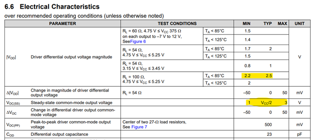
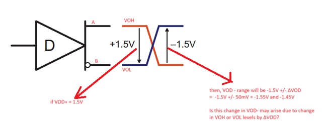
1. The levels VOD, VOC(SS) is marked in the below diagram as per our understanding. Is our understanding correct? Does VOD(pp)-nom = 3V calculated correct?

Ref: Communication Module Reference Design for Functional Isolated RS-485, CAN, and I2C Data Transmission (Rev. A)


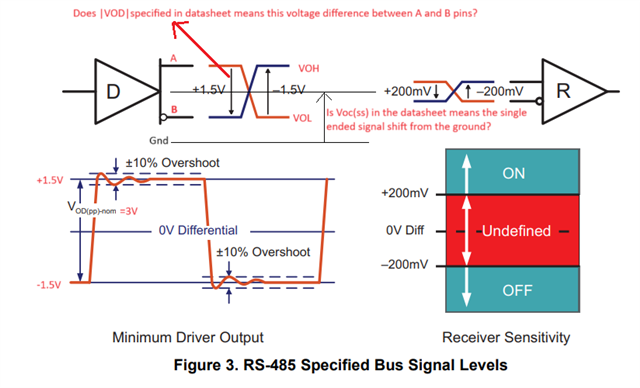
2. Below is the calculation of worst case VOH_min and VOH_max levels (as represented in above diagram), 

    VOH_min = VOC(ss)_min + (VOD_min/2) = 1V + (2.2V/2) = 2.1V

    and VOH_max = VOC(ss)_max + (VOD_typ/2) = 3V + (2.5V/2) = 4.25V. Here, VOD_typ is used as VOD_max value is unavailable.

But, SN65HVD1782-Q1 is connected to VCC = 3.3V and RL = 120ohms (RS-422). In that case, VOH_max is exceeding 3.3V which looks incorrect. Please confirm whether the spec provided is correct or does this calculation is different for VCC = 3.3V?

The |VOD| spec used in the above calculation is for the condition RL=100ohms and 4.75V < VCC < 5.25V.

3. Does VOC(ss) and |VOD| spec different for VCC = 3.3V and RL = 120ohms? If so, is it possible to get the minimum and maximum values of VOC(ss) and |VOD| for the same or do we need to consider VOC(SS)_min = 1V for minimum VCC = 3.15V and VOC(SS)_max = 3V for maximum VCC = 5.25V and |VOD|_min = 2.2V and |VOD|_max = unavailable for the calculations?


  • You understanding is correct. But the datasheet does not specify any maximum values for |VOD|, so it is not possible to compute the worst-case output voltages. You can assume that the range is inside [GND, VCC]. And the overshoot depends on the characteristics of the cable and termination.

  • Thank you for the response

    Q.1 So, can we confirm that the VOC(SS)_min = 1V is for minimum VCC = 3.15V and VOC(SS)_max = 3V is for maximum VCC = 5.25V?

    If so, for a 3.3V operated device, with the available specs, does these calculations make sense?

    VOH_min = 1V + (2.2/2)V = 2.1V and VOH_max= 1V + (2.5/2)V = 2.25V
    VOL_min = 1V - (2.2/1)V = -0.1V and VOL_max = 1V - (2.5/2)V = -0.25V

    But still, it is not within [GND, Vcc]. But marking it as failure doesn't makes sense because the |VOD| spec is for 4.75V < VCC < 5.25V.

    Q.2 Can you please suggest any possible way to map the available spec of |VOD| in datasheet for Vcc = 3.3V?

    We found one datasheet of RS485/RS422 transceiver with VCC = 3.3V. If no way to get the VOD and VOC specs for Vcc=3.3V, can we consider the below highlighted specs for the analysis?


    Q.3 What does delta VOD in SN65HVD1782-Q1 mean? Is this delta VOD normally arise due to differences in VOH (A signal) and VOL (B signal) levels as shown below?

    i.e, VOH (A signal) = VOC(ss) + (VOD/2) and VOL (B signal) = VOC(ss) - (VOD/2) +/- delta VOD


  • Hi Sreelekshimi,

    Sorry for the delay on the response.

    Q1 - your analysis is fine when calculating worst case VOH and VOL - this is basically how we'd approximate more "accurate" boundary conditions as well.  That being said - you probably won't ever see a VOL lower than ground without undershoot/overshoot. The device can't output lower than GND (excluding undershoots) or output higher than VCC (excluding overshoots) - while your analysis is fine because this is absolute worst case simulations and having it be a little worse than reality gives a bit more margin to real systems - in the most technical sense you cannot assume that minimum |VOD| happens at minimum VOC(ss) - i.e. VOC(ss) may be at 1V but |VOD| may be at 2.4V or something similar etc.. 

    Clemens analysis just gives you a short-hand way to avoid doing the extra analysis. The driver can basically attach VCC to A or B with GND attached to B or A - so the most the driver can output at A or B is VCC and the least is ground. During signal transition you could see undershoot/overshoot depending on system setup. 

    Q2- No you have to use theSN65HVD1782-Q1 datasheet to design with this part. If you use a 3.15V supply the typical specifications no longer apply but the device is still bounded by all min/max conditions as described in datasheet. Realistically all designs should be done with min/max only because typical is just to give an idea of standard room temperature behavior - but we don't share variance or anything else so really you shouldn't be designing with typical values (using typical in place of max values when there is no max or using typical in place of min when there is no min is generally okay - but will be slightly less accurate). 

    Q3 - Delta VOD is the difference in the magnitude of differential voltage for different logic values. Ideally the differential magnitude is going to be the same for a logic 1 (A = High, B = Low) and a logic 0 (A = Low, B = High)  - however that isn't always going to happen. So the delta VOD is the difference between differential magnitudes 

    Or in other terms: delta VOD = |VOD(D = H)| - |VOD(D  = L)| = |VOH(A) - VOL(B)| - |VOH(B) - VOL(A)|


    For this device it is to be no more than +/-50mV across operational range. 

    However one important note is that the minimum output |VOD| is the lowest any VOD will be. 

    Please let me know if you have any other questions and I will see what I can do!

    Best,

    Parker Dodson

  • Thank you so for the detailed explanation. No further queries.