Because of the holidays, TI E2E™ design support forum responses will be delayed from Dec. 25 through Jan. 2. Thank you for your patience.

This thread has been locked.

If you have a related question, please click the "Ask a related question" button in the top right corner. The newly created question will be automatically linked to this question.

SN65HVD232: Differential signal interfere

Part Number: SN65HVD232

Hi team 

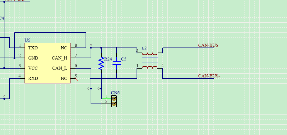
Customer use SN65hvd232 in the single phase inverter, they find when more than one CAN node attached to the CAN network, the differential voltage of CAN_H and CAN_L has some interfere on it, but if there is only one CAN device, the signal is good. Below is the waveform and schematic. 
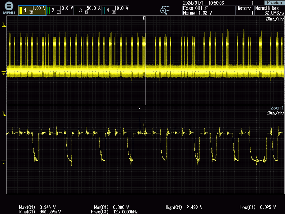
Where should I check for this issue?

thank you 

best regards

joe

  • Hi Joe,

    Just for clarification and to make sure I correctly understand, the waveform you are showing is the differential voltage between the CANH and CANL signals.  Are you using a differential probe connected to the CN6 header I see in the schematic figure? 

    What value is C5 and R24?  Also, why is there not also a resistor between the CANL pin and CN6?  Because CAN is a differential signal, typically you always want equivalent components on both the CANH and CANL pins to make sure they are loaded the same and have the same propagation delay.

    Are the net lengths and trace routing the same for the CANH and CANL signals on the PCB?  If there is a difference in the length or loading of the traces, there could be some skew between the CANH and CANL individual signals that would be visible in the differential voltage.

    Looking at the noise pulses on the signal, this looks very repetitive, and you said this was in a phase inverter application.  What is the frequency of the inverter running at? and what is the frequency of the noise pulses?  Is it the same?

    What do the individual CANH and CANL signals look like by themselves?

    What do the "good" waveforms look like when there is only one CAN device?  However, I don't fully understand how you can only have one CAN device on a bus because CAN requires at least 2 nodes on a bus in order to communicate.  Can you provide more information about what the CAN bus looks like, wiring harness length between CAN nodes and where the termination is located, etc.?

    Does the noise seem to be connected to any one particular board that gets added to the bus, or do all of their boards look good when operated individually, and noisy when added together?

    I would generally recommend trying to look at all signals individually to see if any signal looks like it has noise.  I would also look at the voltage to see if it is picking up the noise which could be getting into the signals through a fluctuating power rail.

    Regards,

    Jonathan

  • Hi Jonathan

    Thanks for your timely reply.

    the waveform you are showing is the differential voltage between the CANH and CANL signals

    Yes.

    Are you using a differential probe connected to the CN6 header I see in the schematic figure

    No, the probe is just common probe with the GND pin connected to CAN_L and signal pin connected to CAN_H, the GND is connected with ground springy, the test point is shown as below together with corresponding schematic:


    What value is C5 and R24

    C5 is 2200pf R24 is 150ohm

    Also, why is there not also a resistor between the CANL pin and CN6

    In the test they connect CN6 with a jumper so that R24 can act as the CAN terminal resistor.

    Are the net lengths and trace routing the same for the CANH and CANL signals on the PCB

    As the PCB shown above, the trace nearly the same.

    What is the frequency of the inverter running at? and what is the frequency of the noise pulses?  Is it the same?

    Yes, after confirmation, the interfere is come from power stage switch.

    What do the individual CANH and CANL signals look like by themselves?

    Please see the pic below, the red line is the calculation result of scope, but the test result is different from calculation.

    What do the "good" waveforms look like when there is only one CAN device?  However, I don't fully understand how you can only have one CAN device on a bus because CAN requires at least 2 nodes on a bus in order to communicate.  Can you provide more information about what the CAN bus looks like, wiring harness length between CAN nodes and where the termination is located, etc.?

    Does the noise seem to be connected to any one particular board that gets added to the bus, or do all of their boards look good when operated individually, and noisy when added together?

    It seems that my expression a little bit confused, "one CAN device" means they test each CAN node individually, the waveform looks good. the case is all of their boards look good when operated individually, and noisy when added together.

    I would also look at the voltage to see if it is picking up the noise which could be getting into the signals through a fluctuating power rail

    Customer feed back that power rail is check, no fluctuate.

    Thanks 

    best regards

    Joe

  • Hi Joe,

    No, the probe is just common probe with the GND pin connected to CAN_L and signal pin connected to CAN_H, the GND is connected with ground springy, the test point is shown as below together with corresponding schematic:

    Using a common single-ended probe in this manner is not usually a good way to look at the differential voltage.  The GND reference of the probe is usually connected to the scope's chassis or earth GND, for most common probes.  Is the GND reference of the probe they are using isolated from the scope's GND?  If not, then the CAN_L signal connected to the probe's GND reference will be shorted to GND and only the CAN_H signal will be seen.

    Please see the pic below, the red line is the calculation result of scope, but the test result is different from calculation.

    If the mathematical difference between the CAN_H and CAN_L signals captured on individual probes does not show the noise pulses, then this shows the noise is coupled onto CAN_H and CAN_L signals equally in the "common" domain.  This means that the noise is NOT in the "differential" domain and it is getting canceled out due to the differential nature of the CAN signals.

    If the noise was only getting coupled onto ONE of the CAN signals and not the other, then this would result in a difference between the two signals that would be visible in the differential domain and seen in the calculated mathematical difference waveform.

    Yes, after confirmation, the interfere is come from power stage switch.

    It appears the noise is coupling onto the CAN_H and CAN_L signal PCB traces or wiring harness through unshielded wires and traces.  I'm not sure I fully understand how the boards are being tested together or individually, but I assume that there is a wiring harness that connects multiple boards together through the CN2 DB9 connector.  If the noise is only present when two or more boards are connected together with a wiring harness, then I would think the noise is getting coupled onto the CAN signals inside the wiring harness. 

    But because this is not visible in the differential domain between the CAN_H and CAN_L signals (as seen in the math waveform) the CAN data will not be negatively impacted by this noise.  This type of noise is why CAN is a differential signal.

    Regards,

    Jonathan