This thread has been locked.

If you have a related question, please click the "Ask a related question" button in the top right corner. The newly created question will be automatically linked to this question.

DS250DF230: Inquiries about Fanout

Part Number: DS250DF230

Hi

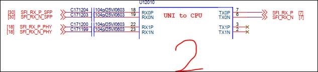
Is the Fan-out method the ability to broadcast signals coming into one port to two ports?
Or are you exporting the signals in two ports to one port?

If it is correct, can you tell me the 'Fan-Out register setting guide' that fits the attached circuit?

Thanks

  • Hi, 

    MUX chip #1 success to configure as fanout (A->A and B) and it works well.

    MUX Chip#1 Fanout Mode.
    i2c write i2c_0 0x18 0xff 0x1
    i2c write i2c_0 0x18 0xfc 0x1
    i2c write i2c_0 0x18 0x96 0x0C
    i2c write i2c_0 0x18 0xff 0x1
    i2c write i2c_0 0x18 0xfc 0x2
    i2c write i2c_0 0x18 0x96 0x03

    However, in case of MUX chip #2, I failed to configure as fanout(?) or mux(?) mode (A and B -> A).

    Please provide a register setting guide that fit MUX #2 circuit, I want to use it without switching channel.

    If it is possible, I'd like to know the register setting value  to configure as 'A and B -> A' on the MUX chip #2.

  • Hi David, DongSeon,

    Fanout refers to mapping 1 input to 2 outputs. Mux refers to selecting between 2 inputs to map to 1 output.

    Your register write sequence to configure fanout is sufficient.

    There are 2 different settings when using the cross-point as a mux:

    • Map RX0 to TX0: use default settings in register 0x96 (ch0 0x96=0x04, ch1 0x96=0x04)
    • Map RX1 to TX0: configure ch1 as a fanout (ch0 0x96=0x03, ch1 0x96=0x0c)

    Since ch1 output is never used, you can mute the output driver by writing 0xa5=0xe0.

    Do you have access to the DS2x0DFxx0 Programming Guide? Although this guide doesn't explicitly have instructions for configuring the cross-point as a mux, it does include register write sequences for many features and configurations.

    Best,

    Lucas

  • Hi Lucas, 

    Thanks reply.

    I have access to the document 'DS2x0DFxx0 Programming Guide'.

    Unfortunately, your register guide not works as i want.

    Connection goes down after setting register you told me.

    I'm confused that register bit should be set one time(0x3&0x4 = 0x07) or two time(writing 0x3 then writing 0x04)?

    Which sequence(#1, #2, #3) of writing register is correct?

    #1 #2 #3
    i2c write i2c_0 0x1b 0xff 0x1
    i2c write i2c_0 0x1b 0xfc 0x1
    i2c write i2c_0 0x1b 0x96 0x04
    i2c write i2c_0 0x1b 0xff 0x1
    i2c write i2c_0 0x1b 0xfc 0x2
    i2c write i2c_0 0x1b 0x96 0x04
    i2c write i2c_0 0x1b 0xff 0x1
    i2c write i2c_0 0x1b 0xfc 0x1
    i2c write i2c_0 0x1b 0x96 0x03
    i2c write i2c_0 0x1b 0xff 0x1
    i2c write i2c_0 0x1b 0xfc 0x2
    i2c write i2c_0 0x1b 0x96 0x0C
    i2c write i2c_0 0x1b 0xa5 0xe0
    i2c write i2c_0 0x1b 0xff 0x1
    i2c write i2c_0 0x1b 0xfc 0x1
    i2c write i2c_0 0x1b 0x96 0x04
    i2c write i2c_0 0x1b 0xff 0x1
    i2c write i2c_0 0x1b 0xfc 0x2
    i2c write i2c_0 0x1b 0x96 0x04
    i2c write i2c_0 0x1b 0xff 0x1
    i2c write i2c_0 0x1b 0xfc 0x1
    i2c write i2c_0 0x1b 0x96 0x07
    i2c write i2c_0 0x1b 0xff 0x1
    i2c write i2c_0 0x1b 0xfc 0x2
    i2c write i2c_0 0x1b 0x96 0x0C
    i2c write i2c_0 0x1b 0xa5 0xe0
    i2c write i2c_0 0x1b 0xff 0x1
    i2c write i2c_0 0x1b 0xfc 0x1
    i2c write i2c_0 0x1b 0x96 0x07
    i2c write i2c_0 0x1b 0xff 0x1
    i2c write i2c_0 0x1b 0xfc 0x2
    i2c write i2c_0 0x1b 0x96 0x0C
    i2c write i2c_0 0x1b 0xa5 0xe0

    And, i want to clarify below comment.

    • Map RX0 to TX0: use default settings in register 0x96 (ch0 0x96=0x04, ch1 0x96=0x04)
    • [DS] Isn't it the default setting value 0x08?

    Thanks.

  • Hi DongSeon,

    • Map RX0 to TX0: use default settings in register 0x96 (ch0 0x96=0x04, ch1 0x96=0x04)
    • [DS] Isn't it the default setting value 0x08?

    Sorry that was my mistake. Register 0x96 default value is 0x08, and this should be written on both channels when mapping RX0 to TX0.

    When using the cross-point as a mux, there isn't a single register write sequence to use. You cannot map both RX0 and RX1 to TX0 at the same time. There are separate register write sequences to be used when mapping RX0 to TX0 and mapping RX1 to TX0. Each time you switch which input maps to TX0, you will need to follow the corresponding register write sequence.

    Since TX1 will never be used on this retimer, I recommend muting the output when you first power up the device.

    • i2c write i2c_0 0x1b 0xff 0x1
    • i2c write i2c_0 0x1b 0xfc 0x2
    • i2c write i2c_0 0x1b 0xa5 0xe0

    When you want to map RX0 to TX0:

    • i2c write i2c_0 0x1b 0xff 0x1
    • i2c write i2c_0 0x1b 0xfc 0x1
    • i2c write i2c_0 0x1b 0x96 0x08
    • i2c write i2c_0 0x1b 0xff 0x1
    • i2c write i2c_0 0x1b 0xfc 0x2
    • i2c write i2c_0 0x1b 0x96 0x08

    When you want to map RX1 to TX0:

    • i2c write i2c_0 0x1b 0xff 0x1
    • i2c write i2c_0 0x1b 0xfc 0x1
    • i2c write i2c_0 0x1b 0x96 0x03
    • i2c write i2c_0 0x1b 0xff 0x1
    • i2c write i2c_0 0x1b 0xfc 0x2
    • i2c write i2c_0 0x1b 0x96 0x0C

    Best,

    Lucas

  • Hi Lucas, 

    I just wanted to know if I could map RX0 and RX1 to TX0 at the same time without switching of channels, as like the fanout.

    I misunderstood the below sentence in the datasheet about mux.

    '1 to 2 fanout, 2 to 1 mux, A to B B to A crosspoint'

    You mean i can't do that.

    I got the answer i wanted.

    Thanks Lucas.

  • Hi DongSeon,

    Yes that's correct, it is not possible to map both RX0 and RX1 to TX0 at the same time.

    Best,

    Lucas