This thread has been locked.

If you have a related question, please click the "Ask a related question" button in the top right corner. The newly created question will be automatically linked to this question.

MAX3221: Powering Issue

Part Number: MAX3221

Hello all!  I was hoping you could shed some light on an issue we are seeing with the MAX3221CPWR transceiver for TTL -> RS232.

For various reasons, one of our design constraints is that the chip must be powered through a 330-ohm pullup to 5V and a Schottky diode (We understand this is not ideal, but it is needed).  And because of the voltage drop that will be present across the 330-ohm when the drivers are drawing current, we have elected to configure the charge pump cap values to work with a VCC between 3V - 5.5V, per the datasheet (C1 = 0.1uF, C2-C4 = 0.47uF).  We have also added some extra bulk capacitance to keep the rail stable, and disabled the auto-powerdown options.  See schematic below:

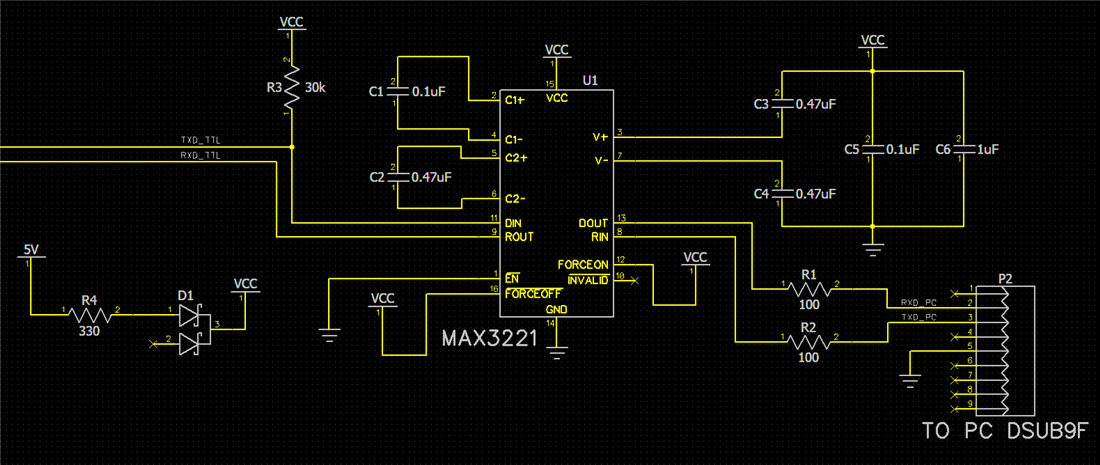
The issue is that when powering this way, the chip will occasionally enter a state where it draws more current than normal, increasing the drop across R4 enough to drop VCC below 3V.  Communication does drop out during this time, and V+ and V- barely reach +/- 3V.  That is with the configuration shown above with C6 = 1uF.  But, if I change C6 to 10uF, the issue goes away entirely.

If it is of any help, these are some measurements from our setup: 

Normal state when communication is active (C6 = 10uF): 

- VCC = 3.7V

- V_D1 = 120mV

- I_R4 = 3.4mA

Issue state when communication is active (C6 = 1uF): 

- VCC = 2.3V

- V_D1 = 190mV

- I_R4 = 7.2mA

One thing we have tried is to delay the start of communication until the pump and bulk caps have charged fully, which we did with RC delay circuits at the EN and FORCEOFF pins, but that did not work.  

Even though the issue seems to go away with more bulk capacitance, I was hoping you might have some insight as to why this happens in the first place?  We wouldn't feel comfortable sending this out in the field if we don't fully understand the root of the issue, and why extra bulk capacitance solves it.  Do note though that if R4 is increased to 410 ohm, no amount of bulk capacitance will fix the issue.

I would also appreciate your opinion on if this way of powering is very unreliable in general, even if working correctly, as knowing it has the potential to have this issue doesn't sit quite right with me.  I cannot repeat the symptom of excess current draw when powering with 5V directly, it only happens when through that resistor.

Thank you in advance,

Thomas

  • Hi Thomas,

    So I do think the issue is how you are powering the device - the voltage drop from 5V is not going to be great as that is going to vary throughout operation and realistically we have this device spec'd for 4.5V to 5.5V or 3V to 3.6V operation - so outside of those ranges we don't really guarantee behavior of device as its outside of our recommended operating range.  I will be transparent here as well - that needs to be changed because any issue with the IC that would be reported from a schematic like this is would be flagged as an application design flaw because really the the VCC pin should be connected directly to the output of a power supply - typically a buck or an LDO - and putting intentional voltage drops between power supply and VCC pin is never advisable especially on a part that will vary on its current draw. 

    1. You have the device setup where it will transmit a signal as soon as power comes on (DIN is tied high, device is enabled) - so its going to be consuming current from the beginning to transmit a signal. 

    2. The issue is that without a larger decoupling capacitor the system doesn't seem to work - this is because the 10uF is acting a charge storage component - it is able to feed more charge to the devices VCC pin - allowing a steady voltage to exist on the bus - the tradeoff is that the system takes longer to start. 

    3. The system very much could consume up to around 5 to 10 mA - the idle no load current alone can go to 1mA on this device - so the 330 ohm resistor is going to be problematic with how the system can vary in its supply current. 

    What I think is happening is that the 10uF is taking a longer time charge than the 1uF capacitor - but when the IC beings to operate (as 10uF is charged to proper level) the capacitor can help reduce needed in-rush current because it has more charge that it can transfer to the VCC pin  - the 1uF capacitor charges quicker but can't sustain the voltage because it has a lower amount of charge. That being said - I wouldn't say the 10uF is a robust solution here - that is a large decoupling capacitor and I am not sure if it would work across operational range of the IC or if it is just working in your test setup - that's why I'd strongly advise redoing the VCC pin design because its in current setup I think you would be able to get it to work - but only marginally and I'd be worried about the robustness of the design. 

    Please let me know if you have any other questions - but I do think it is based on how the system is being powered. 

    Best,

    Parker Dodson 

  • Hi Parker, 

    Thank you for the reply.  I was under the impression from the datasheet that the entire range between 3V and 5.5V was supported so long as the proper charge pump values were selected.  Thank you for clarifying.

    For context, we power this board from external sources, there is physically not enough space for an LDO/buck on the PCB.  We were attempting to make this design compatible with older products that are already out in the field, of which that resistor pullup is the only reference to 5V available externally on the older products.  We would never intentionally choose to power that way, but it is very clear now to avoid this option altogether.

    I do have another question still, assuming we can access a reliable 5V source:

    Cost is a big constraint for this design as well, so we are looking to limit the amount of different parts used.  And now that we are always powering from 5V directly, and never 3.3V, is it still acceptable to keep the charge pump cap values in the 3V - 5.5V configuration?  As we already use 0.1uF for decoupling, so we would only have to add 0.47uF additionally, as opposed to adding a 0.047uF and a 0.33uF for the 5V only setup.

    Thank you again,

    Thomas

  • Hi Thomas,

    Yeah - I understand where the confusion comes from because most of the devices that have a 3V to 5.5V operating range - that usually means the entire range is covered - but this device specifically calls out a 3.3V or 5V supply in the recommended operating conditions table - which they wouldn't do if the entire range was more or less okay to operate in. It shouldn't damage the device - but behavior could be strange and unwanted. 

    That also makes sense working from a legacy system - that would line up why you are trying this supply and to be 100% honest a cursory glance at the datasheet it wouldn't be crazy to read this as a possible option - its one of those very small seemingly innocuous details that can be overlooked pretty easily. 

    For you new question - you can use the 3V to 5.5V range capacitors with either the 3.3V or the 5V supply - it should work fine for both. 

    Please let me know if you have any other questions and I will see what I can do!

    Best,

    Parker Dodson