This thread has been locked.

If you have a related question, please click the "Ask a related question" button in the top right corner. The newly created question will be automatically linked to this question.

DS320PR1601: REDRIVER

Part Number: DS320PR1601

Tool/software:

Hi,

Kindly go through the images below;
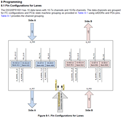
in fig 8-1 as shown in datasheet of DS320PR1601 B_ADDR0 0 to 7(channel 0 to 3) is mapped to bank 0, B_ADDR1(channel 4 to 7) is mapped to bank1.

But in DS320PR1601RSC-EVM User's Guide, B_ADDR0 0 to 7(channel 0 to 3) is mapped to bank 1, B_ADDR1(channel 4 to 7) is mapped to bank0.

Could somebody please clarify this?

Thanks and Regards,

Shekha Shoukath

  • Hi Sheka,

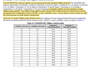
    The two B_ADDR0 and B_ADDR1 pins are configured together to set the address pair for both banks at the same time, I don't think it's accurate to say that B_ADDR0 is mapped to one bank and B_ADDR1 is mapped to another bank because they do not operate independently. Once an address pair (example: 0x18 and 0x19) is selected by the combination of the ADDR0 and ADDR1 pin settings, Bank 0 will be assigned the address with the lower hex value (0x18) and Bank 1 will be assigned the address with the higher hex value (0x19). 

    Best,

    Evan Su