Tool/software:
Hi team,
For out ESD321DYAR, the pin layout is as below
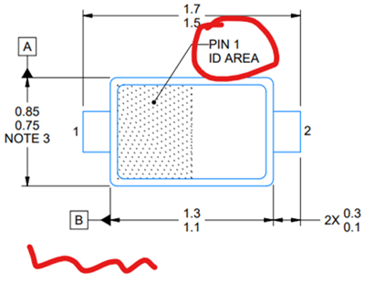
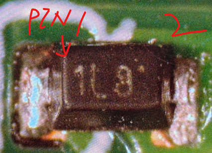
So does that mean the start of the marking '1L8' is the PIN 1, if this understanding is correct?
Thanks
Best regards
Mia
This thread has been locked.
If you have a related question, please click the "Ask a related question" button in the top right corner. The newly created question will be automatically linked to this question.
Tool/software:
Hi team,
For out ESD321DYAR, the pin layout is as below


So does that mean the start of the marking '1L8' is the PIN 1, if this understanding is correct?
Thanks
Best regards
Mia
Hi MIa,
'1L8' is just the device marking.

Pin 1 can be identified by a circulator notch near the lead.

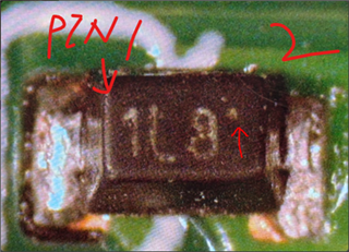
Regards,
Sebastian
Hi Sebastian
Thanks for your feedback.
I would like to double check for two more points here:
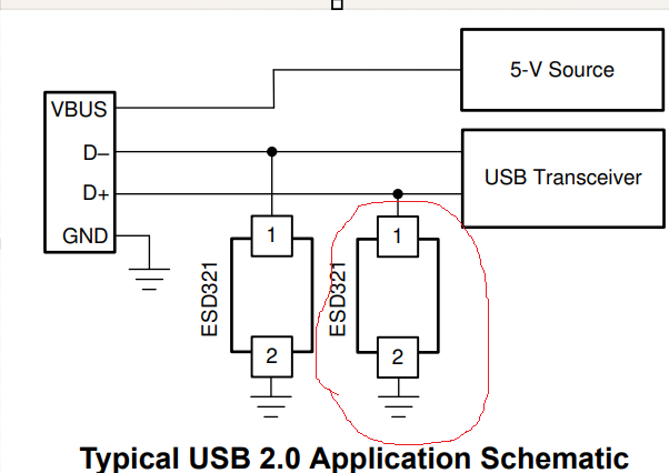
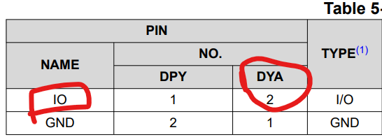
Q1: For sure, for the DYA package, the PIN 2 is the IO pin, and the pin 1 is the GND; the 1st page datasheet is referring to DPY package?
 |
 |
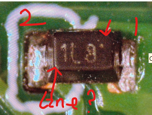
Q2: for the DYA package, does the marking have the line? What does the package in datasheet the ID area means, referring to the circulator?
Thanks
Best regards
Mia
Hi Mia,
Q1: Your understanding is correct, pin 2 will be the input of the ESD diode.
The typical application diagram would be the pinout for DPY not DYA.
Q2: The DYA package will be marked with the circular notch to indicate pin 1, not the line as shown in the package drawing. This was done to avoid issues with the device markings being confused with the line marking for pin 1.
If pin 2 is connected to the data/power line you want to protect as shown in the image, it is connected correctly.
Regards,
Sebastian