This thread has been locked.

If you have a related question, please click the "Ask a related question" button in the top right corner. The newly created question will be automatically linked to this question.

DS110DF1610: CDR Lock challenge depending on MUX config

Part Number: DS110DF1610

Tool/software:

Hi,

We are having difficulty achieving CDR lock in the following condition

We are using the SigCon Architect tool to configure the device and we have a signal input into RX0B

When we have TX0B looking at RX0B we achieve a CDR lock

If we configure TX1A to then look at RX0B we achieve CDR lock on both RX0B and TX1A which makes sense (apart from having not configured master/slave bits)

However if we then configure TX0B to look at an input without a signal and keep TX 1A looking at RX0B (which we know is present) we loose both the SD and CDR for TX0B but also loose the CDR on TX1A?.

If we then configure TX0B to look at RX0B again, we get CDR lock on both TX0B and TX1A, 

Can you tell me the correct way to reroute a one to one configuration so that you can achieve a CDR lock when your output channel is not the same as the input channel?

Thanks,
Dave

  • Hi Dave,

    Are you configuring the crosspoint with the Crosspoint Switch Tab on the High Level Page? Or are you directly reading/writing registers on the Low Level Page?

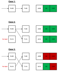
    I created a diagram based on my understanding of your observations. Is my understanding correct?

    If my understanding is correct, then in case 3 it is expected behavior that ch0B indicates no signal detect and no CDR lock. This is because ch0B status registers will report on the Rx1A --> Tx0B signal path. It is unexpected that ch1A indicates no CDR lock. ch1A should indicate signal detect and CDR lock because its status registers report on the Rx0B --> Tx1A signal path.

    Please let me know how you are configuring the crosspoint and I can share debug recommendations.

    Best,

    Lucas

  • Thanks for the quick response.

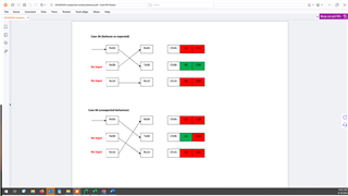
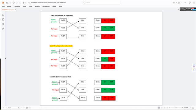
    The case 3 that you drew above is as expected in that that we do get both a CDR lock and SD indications for Tx1A, the case that doesn't behave as expected is the attached scenario (See attached Case 3A/4A). In fact this behaviour appears any time there isnt some sort of reciprocity in the routings ie if Rx1B is routed to TX1A then unless RX1A is routed to TX1B it will not CDR lock. The unexpected behaviour changes somewhat if there are signals present on the other inputs...for example if a signal was present on Rx1A below then both Tx0A and Tx0B would provide a CDR lock.

  • Oh, and we are using the SigCon Architect tool to generate these configurations, we are in the process of developing our routing code and using SigCon to confirm the routings should work.

  • Yes, these configurations were set up using the Crosspoint Switch Tab on the High Level Page.

  • Hi Lucas, for clarity I've regenerated my drawing to include the additional case I described above, where a signal is present on Rx1A, see Cases 3A/4A/5A below. Case 3A and 5A behave as expected, however case 4A does not, the only difference between 4A and 5A is that there is an additional signal present (Rx1A). The physical routing is identical between 4A and 5A...

  • Hi David,

    Thank you for your detailed clarifications on your setup cases and SigCon configuration method. I agree that it is unexpected behavior for the Rx0A/Tx0B signal chain to lose CDR lock in case 4A.

    Allow me to try to reproduce this behavior in a bench experiment. I'll need some extra time to work on this so I'll target completion by end of this week and get back to you with feedback.

    Best,

    Lucas

  • Hi David,

    I was able to reproduce this behavior in a bench experiment. When I configured the crosspoint as shown in case 4A, I also saw ch0B lose lock. After investigating register values, I found there is a bug with the Crosspoint Switch tab on SigCon Architect.

    There are 2 registers that are used to control the crosspoint: 0x96 and 0x9B.

    • 0x96 is programmed from the perspective of the Tx side. Bits 1:0 are used to determine which Rx channel should connect to the Tx side. For example, ch0 reg 0x96=0x1E means Rx1A will be connected to Tx0A. Note that bits 4, 3, 2 need to be asserted to properly enable the crosspoint.
    • 0x9B is programmed from the perspective of the Rx side. Bits 1:0 are used to determine which Tx channel should connect to the Rx side. For example, ch2 reg 0x9B=0x00 means Rx1A will be connected to Tx0A.

    When the crosspoint is configured from the Crosspoint Switch tab, register 0x9B values are programmed incorrectly. SigCon assumes 0x9B is programmed from the perspective of the Tx side, which is incorrect.

    The table below shows register values for case 4A. Incorrect 0x9B values were programmed by the Crosspoint Switch tab configuration. After I changed 0x9B registers to the correct values, ch0B correctly showed CDR lock.

    Channel 0x96 Value Incorrect 0x9B Value Correct 0x9B Value
    0A (0) 0x1E 0x02 0x01
    0B (1) 0x1C 0x00 0x02
    1A (2) 0x1D 0x01 0x00

    Despite the bug, the Crosspoint Switch tab still programs register 0x9B values correctly in fanout and A->B/B->A crossing configurations. The Crosspoint Switch tab can still be used as a starting point for configuration, however I recommend always reviewing register values to confirm if they are programmed correctly.

    Best,

    Lucas

  • Hi Lucas,

    I work with Dave, he is on vacation right now so he is unable to reply. We tried out your solution and it seems to have fixed our issue, thanks!

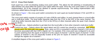
    Also just an FYI, I think the cause of our confusion was a misunderstanding of semantics at the following section of the datasheet (highlighted and shown below). We assumed that the use of the word "mirror" meant to "copy" or to "be the same as", which was incorrect.

    Although, now that we know what the issue was,  I can now also see the word "mirror" being interpreted as "a mirror reflection", as in the channel register 0x96 (TX perspective) needs to be a "mirror reflection" of channel register 0x9B (RX perspective). Maybe this was the way it was meant to be interpreted? 

    However I think your explanation on how to program channel registers 0x96 and 0x9B was much more clear. Maybe in the future this section of the datasheet could be updated to be more explicit about channel registers 0x96 & 0x9B, just to eliminate the possibility of being misinterpreted like in our case.

    Thanks again for solving our issue!
    -Kyle

  • Hi Kyle,

    Great, I'm glad I was able to clear things up! You're right that the wording in the datasheet is a bit misleading. We have this noted down and plan to make edits for the next datasheet revision.

    Best,

    Lucas