This thread has been locked.

If you have a related question, please click the "Ask a related question" button in the top right corner. The newly created question will be automatically linked to this question.

TUSB1002: TUSB1002

Part Number: TUSB1002
Other Parts Discussed in Thread: , TUSB1104, TUSB1004, TMUXHS4612

Tool/software:

Dear Sir/Madam,

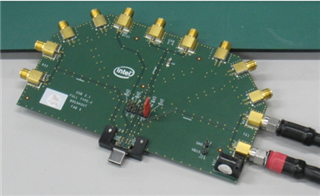
We are using TUSB1002 Linear Re-driver part for our USB3.2 Gen2x2 FMC Card. We have our own USB3.2 IP Core. 

Right now, board is under testing. 

Before playing re-driver setting, I would like to have detail understanding of below terms with respect to waveform effect.

How can we repair Tx and Rx side signals with these parameter settings?

1. VOD 

2. Equalizer Gain

3. DC Gain

I have tried to find similar articles and app notes available on TI but now found useful information. 

Please guide us at the earliest. 

  • Hi, thanks for reaching out. These settings can be used to recover a USB3 signal from excessive trace loss.

    1. VOD will alter the linearity range of the TUSB1002. The linearity range is the acceptable swing of the input signal for our device on the RX1/RX2 pins. Increasing this value to 1200mVpp is typically the best starting setting.

    2. EQ gain will boost the high-frequency AC component of the signal to account for insertion loss on the receivers of the TUSB1002A. A simple way to think about this is that the longer your channel length/more channel loss you have on the receiver of our device, the higher EQ setting you need to compensate the channel. If you know the channel loss before and after the TUSB1002, I can help recommend a starting EQ setting. I recommend looking at this E2E FAQ.

    3. DC gain will boost the low frequency AC component of the signal. This is typically best to keep at 0dB when beginning testing. If you need extra boost on the low frequency signal swing to get your signal to pass compliance, consider increasing the DC gain to +1 or +2.

    When designing a re-driver in your system, its best to install both pullup and pulldown options on all EQ and CFG pins. This allows you to change settings as-needed when verifying the design.

    Best,

    Shane

  • Dear Shane,

    Thank you very much for your valuable guidance. 

    Can you please provide waveforms pictures to showcase of all three features (1) VOD (2) EQ Gain (3) DC Gain?

    It will help me lot to understand and visualize these features effects.

    Also share me application notes, white papers Or Book to more understand it in depth.

  • Dear Shane,

    Regarding VOD, correct me if I am wrong, it is maximum differential input voltage limit which Re-driver can safely accept.

    It has nothing relevant to Amplitude increment-decrement. 

    Please confirm. 

    Also share your valuable guidance on my last weekend queries mentioned below.

    **********************************************************************************************************************************

    Can you please provide waveforms pictures to showcase of all three features (1) VOD (2) EQ Gain (3) DC Gain?

    It will help me lot to understand and visualize these features effects.

    Also share me application notes, white papers Or Book to more understand it in depth.

    **********************************************************************************************************************************

  • The waveforms for these features can be found in the TUSB1002 datasheet:

    VOD linearity setting: 

    EQ gain curves: 

    DC gain: 

    I recommend looking into these app notes for a better understanding:

    1. Linear Redriver Signal Conditioning Theory and Practical Tuning Method

    2. Create an Eye opening Experience with a 10G USB redriver

    Regarding VOD, correct me if I am wrong, it is maximum differential input voltage limit which Re-driver can safely accept.

    Short answer is yes. VOD is the linearity range that our redriver can accept at the input and convert to a 1:1 output. With a small linearity range, signals will get compressed at higher differential input voltages and the output will no longer look 1:1 with the input. Keeping the maximum VOD setting gives our re-driver the best chance at keeping the input and output signals 1:1 with each other:

    Best,

    Shane

  • Dear Shane,

    Thank you so much for giving us valuable insight. 

    Somehow, I am not understanding VOD Setting up to now. 

    As per above attached image, by increasing VOD Setting Eye opening is much wider and cleaner. 

    I may mis-interpret higher VOD Setting with higher Gain figure, which is not true. Does it mean higher VOD setting give higher amplitude waveform?

    I am bit new in this so my questions might be silly but please kindly guide me with respect to attached above VOD setting waveforms. 

  • It is no problem, the VOD setting can be difficult to understand. You are correct that VOD and gain are two separate settings.

    Does it mean higher VOD setting give higher amplitude waveform?

    A higher VOD setting may give a higher output amplitude, but it really depends on the input amplitude. For example (looking at the datasheet chart) an input amplitude of 0.2V to 0.6V is well within the linear range for all VOD settings, so it would be ok to use any VOD setting. In this case, you probably wouldn't notice any output amplitude change in the signal regardless of the VOD setting:

    Once you increase the input amplitude beyond 0.6V, notice how the 900mV VOD setting begins to compress the output amplitude. This is because the signal is going beyond the linear range of that setting, which will shorten the eye opening. In this case, its better to use a higher VOD setting so the signal is not compressed with a higher input amplitude.

    In general its best to leave the VOD setting at the maximum value. This gives our device the best linear range.

    Best,

    Shane

  • Dear Shane, 

    Thank you very much for valuable explanation. It helps us lot to learn Re-Driver. 

    Is it possible for TI team to support us waveform measurement of Super-Speed LANE (10Gbps)?

    It will be great help from TI if they can support us to check eye pattern for various equalizer and DC Gain settings. 

    We will ship our FMC Cards with ALTERA/Intel Host Boards to TI Technical center USA/UK/INDIA. 

    We are ok even if support is chargeable from TI. 

    Kindly connect us with respective technical division of TI for Test and Measurement Support. 

  • Unfortunately, we do not have the resources to accommodate the testing you describe. Typically customers use a test house such as Granite River Labs (GRL) to perform USB compliance testing, so I recommend taking this approach. They have locations worldwide for testing.

    Furthermore, I'd like to re-visit your original system proposal. You are making a USB3.2x2 FMC card correct? I want to highlight that the TUSB1002 does not support x2 mode. Consider using the TUSB1104 for this purpose.

    If you have any questions on the TUSB1002 or TUSB1104 I'm happy to help.

    Best,

    Shane

  • Dear Shane, 

    Thanks for your supportive response. We will surely contact Granite River LABs. As far as my knowledge generally, such type of LABs will provide us equipment to play rather than providing expert guidance like you to modify Redriver Settings meaningfully. 

    That's why our technical management was expecting that TI will provide chargeable technical support. 

    Regarding TUSB1002 usage for USB3.2 Gen2x2 mode, actually we have used 2x TUSB1002 Redrivers to run our card in USB3.2 Gen2x2. 

    Is it right design approach? We would like to know your valuable insight here because we are redesigning our same card for few minor modifications requested by our client. 

    Our technical team is wondering that utilizing 2xRedrivers for USB3.2 Gen 2x2 mode create timing violation and fails us till date in this testing.

    Is it main root cause behind failure? Can we pass compliance testing with 2xTUSB1002 Redriver with USB3.2 Gen2x2?


    Does 1xUSB1004 is right decision in this case?

    Please provide detail guidance in this regard. 

  • Using two TUSB1002 devices will not work for USB3.2x2 mode because each TUSB1002 will operate off of an independent state machine. In USB3.2x2 mode, one lane is set as the configuration lane and the other lane must follow the lead of the config lane. This is handled by the TUSB1104 but cannot be implemented with two TUSB1002 devices because there is no internal logic for setting config/follow lanes.

    You can read more about USB3.2x2 mode in the TUSB1104 datasheet:

    Is it main root cause behind failure? Can we pass compliance testing with 2xTUSB1002 Redriver with USB3.2 Gen2x2?

    It is likely that compliance will fail for USB3.2x2 mode if you are using two TUSB1002s.

    Best,

    Shane

  • Dear Shane,

    Thank you very much for your valuable support. 

    In my past few communications, I have mentioned TUSB1004 mistakenly. You have suggested TUSB1104. We will definitely go with your suggestion. But for my knowledge, I would like to know what the basic functionality difference between TUSB1004 is and TUSB1104 because both are 4-Ch Redrivers. 

    One last support I require from your side. 

    I would like to purchase technical book to understand Redriver setting like EQ Gain, DC Gain, Pre-emphasis, De-emphasis, DFE tapping, Clock Data Recovery etc. because at this point you have given us very good knowledge of Redriver setting of EQ Gain, DC Gain and VOD but from Intel/ALTERA FPGA is offering us plethora setting of Signal Conditioning inside FPGA Mega Core function features. 

    I need to understand all these settings and their significance from practical waveform effect perspective. 

    So please suggest us book (highly preferable option for me for detail study) and App notes/white papers as much as possible. 

  • A good resource I've used to learn about signal conditioners are the TI precision labs signal conditioner video series. This covers the basics of re-driver settings and eye diagrams.

    For PCB design with high speed signals, consider the book: High Speed Digital Design by Howard Johnson and Martin Graham

    Aside from this, you can look at our re-driver products and find technical articles, app notes, and white papers that cover signal conditioning and more specifically USB interfaces. These can be found in the 'Technical documentation' section of any product page:

    A few app notes worth looking at for your application are:

    1. USB3.2 Dual lane operation

    2. Strengthening the USB Type-C Signal Chain through re-drivers

    If you have more specific questions on our parts, feel free to reach out over E2E.

    Best,

    Shane

  • Dear Shane,

    Thanks a lot.

    My below query was unanswered. Please guide me.

    *********************************

    In my past few communications, I have mentioned TUSB1004 mistakenly. You have suggested TUSB1104. We will definitely go with your suggestion. But for my knowledge, I would like to know what the basic functionality difference between TUSB1004 is and TUSB1104 because both are 4-Ch Redrivers. 

    *********************************

  • The difference is that the TUSB1004 uses two separate state machines that do not communicate with each other. This would be equivalent to using two TUSB1002s, where each port is independent of the other.

    In summary the TUSB1104 supports USB3.2x2 mode, the TUSB1004 does not.

    Best,

    Shane

  • Dear Shane, thank you so much..

    I am studying your suggested app notes.

    Why high EQ gain setting sometimes degrade eye pattern instead of improvement?

    Also I observed that higher DC Gain is degrading lower frequency components. DC Gain=0 is giving good results instead of DC Gain=+2.

    Can you please share your guidance and experience in this regards?

  • Let me help explain:

    Why high EQ gain setting sometimes degrade eye pattern instead of improvement?

    Its possible to over-equalize the signal by applying too much EQ. When you over-equalize the signal, it will add jitter that can degrade the eye when viewed through a scope.

    Also I observed that higher DC Gain is degrading lower frequency components. DC Gain=0 is giving good results instead of DC Gain=+2.

    DC gain will apply EQ gain to low frequency components of the signal. Keep in mind that lower frequency signals do not incur as much loss as high frequency signals, so there is often very little loss on the low frequency component of signals. This means it does not take much equalization to over-equalize the signal at low frequencies. In general, I recommend starting with DC gain = 0 before applying DC gain.

    Best,

    Shane

  • Thank you so much Shane for your valuable technical help. 

    Your answers are clearing my doubts effectively. 

    I have asked team to prepare schematic page with TUSB11104. It will take couple of days.

    Would you please help us and check our schematic page of TUSB1104? It will help us to move quickly. 

    Regarding my request of handbook of equalization of high-speed signals, I found various articles shown below.

    If you found special handbook, please share book title. 

    Resonant Free Power Network Design (ntu.edu.tw)

    http://emlab.uiuc.edu/ece546/Lect_27.pdf

    An Introduction to Preemphasis and Equalization in Maxim GMSL SerDes Devices | Analog Devices

    Test Happens - Teledyne LeCroy Blog: Introduction to Channel Equalization

    Microsoft PowerPoint - Lect 9 Equalizers (yonsei.ac.kr)

  • Dear Shane, 

    As per my recent communication with Granite River LAB technical team, they don't have probe/fixture to directly probe on AC Coupling Capacitors pads to see the signals at RX end after Re-Driver. They have UXR0334A, 33GHz, 4-Ch. Oscilloscope model. All 4-Channels have 50 Ohm input impedance.

    They have ready SMA Probe channel cables with matched 50 OHM Impedance. As we are redesigning our board for TUSB1104, my technical management is asking me to put on-board SMA Connector support on Redriver Input and Output side to monitor Super-Speed Signals and Eye-pattern analysis.

    Do you have proven reference design to put SMA Connector as a signal tapping points on Super-Speed Lanes without compromising/loading Super-speed lane performance?

    It will be great help for me. 

  • Would you please help us and check our schematic page of TUSB1104? It will help us to move quickly.

    Certainly. I'm happy to review the schematic and point out any changes/recommendations. You can post the schematic here on the public forum, or you can privately direct message me the schematic by accepting my friend request on E2E. In either case, please share the schematic as a PDF file if possible.

    Do you have proven reference design to put SMA Connector as a signal tapping points on Super-Speed Lanes without compromising/loading Super-speed lane performance?

    The closest reference design I can think of is our TMUXHS4612 EVM which uses SMP connectors as breakouts. The schematic and layout images for this board can be found in the associated EVM User's guide.

    GRL may have a USB-C Breakout fixture that converts the Type-C port to SMA headers. The measurement wouldn't be taken directly from the AC coupling capacitor pads, rather it would be taken from the USB-C port with this fixture. This is one way to measure signal quality on a USB-C port:

    Best,

    Shane

  • Dear Shane, 

    Thank you so much for your continuous support.

    We have checked TMUXHS4612 EVM Design. It will be useful in our upcoming application but not helpful in our present case as we need to probe the Super-Speed LANE Signals via SMA Connector during live communications. Important condition is that LANE Performance must not be affected due to signal tapping via SMA Connector. 

    I have attached image of Keysight probe head PCB Zif tips for your easy reference. This is kind of similar tool arrangement which we need via SMA Connector. This PCB Zif Tips are soldered on pads and give us live performance eye pattern. 

    Actually, we need to observe the Superspeed Lane signals in Rx Card at Redriver Output during actual communication is going on as per PRBS sequences. 

    In parallel, you can share Reference Design of USB Type-C Breakout fixture (10Gbps) that converts the Type-C port to SMA header.

  • Unfortunately I don't have the design for that fixture. Its a commonly used USB-C compliance fixture produced by Wilder technologies. You can find the fixture here: https://www.wilder-tech.com/en/products/usb31 

    I'll keep an eye out for the schematic. In the meantime let me know if you have any questions on the TUSB1104.

    Best,

    Shane

  • Dear Shane, 

    Thanks for your support. 

    Regarding net length matching criteria in USB3.2 Gen2x2 can you please check our below understanding. 

    - Net Length of all SSTX pairs need to be matched

    - Net Length of all SSRX pairs need to be matched

    - There is no necessity to match Net Length between of SSTX and SSRX pairs. I need to say that SSTX (Length) = SSRX (Length) is not required in USB3.2 Gen 2x2 communication. 

    Your valuable guidance will be very helpful. 

  • You have the right idea. For USB lines, you need to match the p/n lines within each TX/RX pair. For USB3.2x2 mode, its best to match the SSTX1/2 and SSRX1/2 pairs as well. There is no requirement to match SSTX1 to SSRX1 or SSTX2 to SSRX2.

    Best,

    Shane

  • Dear Shane, 

    During checking of Impedance between P and N lines of Tx Pair of TUSB1002A, it is showing around 96 OHM. Is it OK?

    Because between P and N lines of Rx Pair of TUSB1002A, it is showing impedance in the range of Mega OHM. 

    We have checked above impedances on board as well as on stand-alone chipset of TUSB1002A and Impedance values are mentioned as above.

    Please confirm that these Impedance values are OK. I want to just check that TUSB1002A parts are OK from usage perspective or not because they are purchased before 1 year and we are using it right now. 

    Does these impedance value correct? TUSB1002A is showing proper Impedance values and OK to use in circuit Or TUSB1002A is degraded and not usable and need to use new fresh TUSB1002A?

    Please guide us.

    PS- I have dropped a private email to you about board design review. Kindly check it and let us know your valuable feedback.

  • Dear Shane,

    Regarding Impedance matching of Super-Speed Lane on our FMC Card, what Impedance value we need to match? Is it 90 OHM +/- 10% Or 100 OHM +/- 10%?

    Because as per USB Specification, we need to follow 90 OHM Impedance matching criteria but while checking FMC Carrier Card developed by Intel/ALTERA, they are maintaining 100 OHM Impedance matching Criteria. That's why we are wondering about what Impedance value we need to follow for Super-Speed High Speed Lanes of USB3.2 Gen2x2 communication.

    Please provide us your valuable insight. 

  • Hi Himanshu,

    96 OHM differential impedance is ok for the high speed signal pair. We typically recommend 90 ohm +/- 10% for the differential impedance:

    Because between P and N lines of Rx Pair of TUSB1002A, it is showing impedance in the range of Mega OHM. 

    Are you measuring this while the TUSB1002A is connected to a USB host and device? The 1002A needs to detect the presence of a host and device before it will enable terminations on the RX lines. If you measure the RX lines without anything connected, there will be no terminations. The TX lines will always have terminations enabled.

    If you are still seeing mega ohms of impedance when the TUSB1002A is connected to a device and host, then there could be an issue with the layout or with the specific TUSB1002A device you're using. I would try another TUSB1002A to confirm whether this is the issue.

    what Impedance value we need to match?

    I recommend using 90 ohm +/-10% for the differential impedance. This is the recommendation from the TUSB1104 datasheet.

    Best,

    Shane 

  • Dear Shane,

    Yesterday I have forgotten to share our results of impedance measurement of Tx and Rx lanes between P/N Lines.

    We have measured impedances with FMC Card Turn ON condition with Enumeration successful. 

    We got 89 OHM Impedance between P/N lines of Rx

    We got 75 OHM Impedance between P/N lines of Tx

    Kindly provide your view and let us know if any further measurement will be needed. 

  • Hi Himanshu,

    Its good that the enumeration is successful, but the impedance on your TX lines is low. This impedance should be between 81 Ohms and 99 Ohms (90+/-10%). Can you double check the TX impedance measurement?

    If 75Ohms is the differential impedance, I recommend adjusting the trace to raise this within the 90 +/-10% range. Having a differential impedance as low as 75Ohms can cause issues with enumeration.

    Best,

    Shane

  •  Dear Shane, 

    As per my discussion with Layout Engineer, we would like to know net-length matching mechanism. 

    Option-1 -> Do we need to match Net-Length between Tx Pairs stage by stage.

    Or

    Option-2 -> Do we need to only match Net-Length between Tx Pairs end to end i.e. USB Type-C Connector to FMC Connector? Same question for Rx Pairs.

    Please refer attached image for your easy reference. 

  • Hi Himanshu,

    Option 2 is correct here. You do not need to match SSTX1/2 at each point in the design, but they should match from end-to-end.

    Best,

    Shane