This thread has been locked.

If you have a related question, please click the "Ask a related question" button in the top right corner. The newly created question will be automatically linked to this question.

TPS54678: Load transient leads to large ripple

Part Number: TPS54678
Other Parts Discussed in Thread: DS560DF810, TINA-TI

Tool/software:

Hi,

I have a board with TPS54678 that powers a DS560DF810.  Whenever I perform a soft reset on the DS560DF810 device, I observe the output of the TPS54678 starts oscillating and the power good pin state toggles.  A soft reset of the DS560DF810 results in a load step where current decrease from ~2.5A to ~0.5A, so roughly a -2A step.

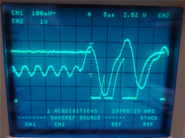
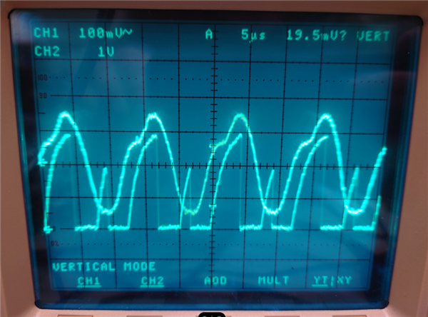
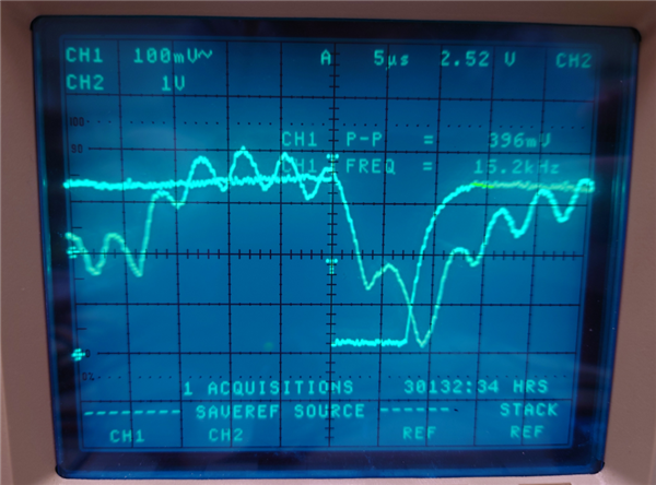
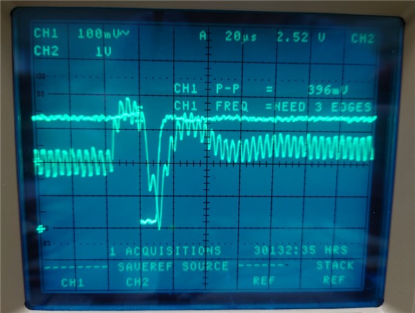
I'm not sure if the magnitude of the ripple shown in these scope captures is accurate, did not probe with tip/barrel method.  However, I think this shows power good output correlates to exceeding Vout thresholds.

Initial transient resulting in this behavior:

  • CH1: Vout, AC coupled
  • CH2: Power good, DC coupled

"Steady state" behavior of Vout after load step:

  • CH1: Vout, AC coupled
  • CH2: Power good, DC coupled

Can you help advise on how this can be resolved?  Is this something that could be due to the compensation network or a lack of Cout?

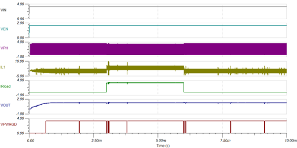
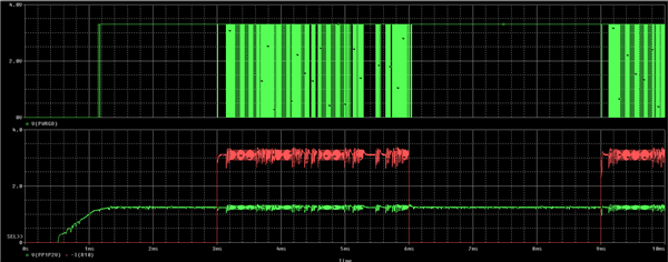
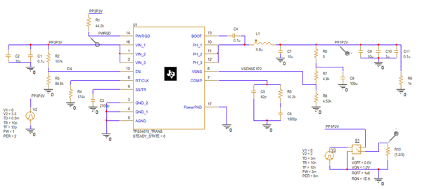
I've also worked on simulating this, but I'm seeing conflicting simulation results between tina-ti and pspice when it comes to the power good state and how load steps are handled.  Please let me know if you have any thoughts on the simulation discrepancy.  Neither simulation shows this "oscillation" behavior observed on the board.

Tina-TI

Pspice
Thanks,

Drew

  • Hi Drew,

    thank you for providing a detailed issue report. A 2A drop should not cause any issues on this device. Is the PSpice schematic identical to the used HW?
    I will review this case and come back to you later this week.

    Regards, Werner

  • Hi Werner,

    Thanks for looking into this.  I will email you the complete schematic (it is not public), but the PSpice schematic is similar to hardware.  Of course, PSpice is using resistive load.  I'm wondering if non-linear load behavior of DS560DF810 may be contributing to this issue.

    Thanks,

    Drew

  • Hi Drew,

    thank you for providing the schematics.

    Both the input and output capacitance seems very low to me, if you compare it with the example of the datasheet. How did you calculate those? Can you try adding more capacitance to both sides?

    Also, do you have the calculation of the compensation network?

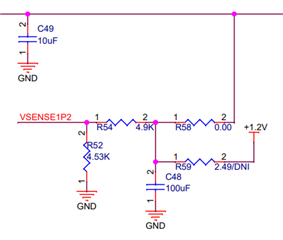
    Your Vsns line seems to miss one capacitor, C15 in the datasheet.

    Please review the compensation, it seems to me that this setup is unstable and the reason for the observed behavior.

    Regards, Werner

  • Hi Werner,

    Thanks for reviewing our schematic.  I did not design this DC/DC converter, so unfortunately I don't have details on the calculations for input/output capacitance and compensation network.

    Additional investigation of the boards I have shows that for some reason, the 100 uF capacitor on Vout is not populated.  This is inconsistent with schematic/BOM, so this was surprising to me.

    I've observed that by adding 100 uF capacitor, PWRGD still drops for a short period of time during this load step, but the output now recovers.

    Negative load step response after adding 100 uF capacitor:

    • CH1: Vout, AC coupled
    • CH2: Power good, DC coupled

    From my side, I think the issue is closed.  I can re-open the thread if something comes up.  Thanks for your help!

    Thanks,

    Drew

  • Thank you for reporting your findings.

    Even with the 100uF populated, the total Cout is still very low. The example in the datasheet uses 5*47uF=235uF.

    Adding further output capacitance and fixing the Vsense network will increase the operation even further. Power good should be okay during the whole transient. More Cin might also be required for stable operation.

    Regards, Werner

  • Hi Werner,

    Thanks for your feedback.  We will continue to look into this.

    In the data sheet example, they calculated Cout of 73uF (equation 20), but then increased this ~3x to 235uF.  Using the same equation with 0.8uH inductor instead of 1.2uH, I calculate 48uF Cout.  So we'd have ~2x minimum Cout based on equation 20.  Do you think this is sufficient?  Is there a typical scaler for how much more capacitance is added beyond data sheet calculations?

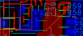
    On my side, I'll also try 200uF (waiting on some parts for this) to see how this impacts converter behavior.  I also observed that layout of C48 does not seem optimal.  There is just a small trace connecting R58 to C48 and this needs to conduct close to 4A p-p ripple current.  I'm planning to try adjusting capacitor location to seem impact of this layout feature.

    Regarding the feedback network, are you able to comment on specifically how C15 is expected to impact load step behavior?

    Thanks,

    Drew

  • Hi Drew,

    the calculated capacitance is for ideal capacitors. You'll need to add more than that with real capacitors because of degrading like DC bias, temperature, aging, etc. The exact numbers depend on your specific capacitor, but going 2x or 3x is not rare, if you have the board space. Improving the layout can also help a lot, please review chapter 10 of the datasheet.

    8.2.2.4

    Additional capacitance de-ratings for aging, temperature and DC bias should be factored in which increases the
    minimum value calculated in Equation 20. For this example, five 47-μF 10-V X5R ceramic capacitors with 3 mΩ
    of ESR are used. The estimated capacitance after derating is 5 × 47 μF × 0.9 = 211.5 μF.

    Regards, Werner