This thread has been locked.

If you have a related question, please click the "Ask a related question" button in the top right corner. The newly created question will be automatically linked to this question.

TUSB1002A: Design feasibility check

Part Number: TUSB1002A
Other Parts Discussed in Thread: TUSB1142

Tool/software:

For inhouse testing purpose I need to switch USB 3.1 signals and power delivery between two sinks.

I did a design using 4 passive switches, controlled and monitored by an MCU.

It basicly behaves as one just would plug the whole cable to the desired output.

The signal switching part seems to work as intended, but I assume, the signal degradation is an issue in my setup. I don't have an scope fast enough to verify.

So the signal chain now looks as follows:

(HOST) -- (USB C to USB C passive Cable 1m) -- (SWITCH PCB) -- (USB C to USB C passive Cable 1m) -- (DEVICE)

After checking the USB 3.x standard for 10Gbps only allows for 1m of cable in the signal chain.

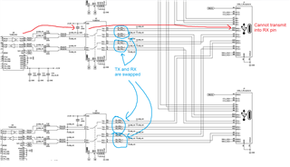
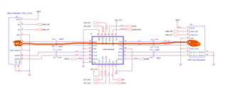
So I did a redesign of my circuit and added two TUSB1002A to the high speed signals to boost the signal. 

My questions:

1. Is it possible to use the TUSB1002A in this application?

2. Did I wire in the TUSB1002A in the correct way?

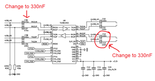
3. For my understanding it should be okay to change the 330nf coupling capacitors to 470nf, am I wrong?

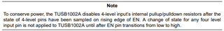
4. As I understood the configuration pins only get sampled on EN rising edge. Due to lack of available GPIO I tied all the configuration pins of the two TUSB1002A togther. They only have individual gpio for the EN lines. I plan to configure them one after the other triggered by the EN line. Will there be any issues doing so?

5. Are there any issues in general with my layout of the high speed signals? I routed them as differential pairs with 90 Ohms impedance, solid copper under the traces as reference plane. Not clear about my layout of the pull-down resistors on the 470nf coupling capacitors (R14/R15 , R35/R36) can this be done better?

Attached is schematic of the switching circuit and the boards copper layers. and a screenshot of the PCB

I would be happy if I could get some feedback.

Switch-Matrix-SCH.pdfSW-USB__Assembly.pdf

  • Hi Benjamin,

    Thanks for reaching out. I'll take a look at the schematic and stack up to see if I find any issues.

    To answer your questions:

    1. The TUSB1002A can compensate for insertion loss from the cables. You might also consider using the TUSB1142, which integrates the MUX + re-driver into one IC.

    2. Let me follow up on this one

    3. You need to keep capacitors on the RX lines between 297nF to 363nF. I do not recommend using 470nF on the RX lines.

    4.Yes this should be ok. The TUSB1002A will only sample on the rising edge of EN, so you could set all config pins for device 1 --> let EN rise for device 1 --> change the config pins to the device 2 settings --> let EN rise for device 2.

    Just make sure you follow the setup and hold timing requirements for the TUSB1002A:

    5. Let me follow up on this as well. In general its better for us to review layouts as a cadence (.brd) or altium file. A PDF will not show details such as trace lengths, dielectric thickness, and footprint sizes.

    Best,

    Shane

  • Hi Benjamin,

    USB-C receptacle to USB-C receptacle is not a typical use case for our parts so my support will be limited. I'll focus on the signal conditioning aspect of this design and leave the Type-C negotiation (CC1/CC2) to you.

    Your design looks to operate similarly to an active cable. The TUSB1002A uses fixed EQ settings that cannot dynamically change to account for channel length/loss changes. In this case, you should keep a dedicated set of cables before and after the board. Switching cables after tuning our EQ may cause our TUSB1002A to over equalize or under equalize the signal depending on the loss change between cables. If you need the ability to change cables, consider using a re-driver with adaptive-EQ or a retimer.

    You've got the transmitters from our 1002A connecting to the RX lines on the right-side USB-C receptacles. You cannot transmit into the RX paths as these are meant to receive signals from the receptacle. You will need to connect the RX lines on the right hand receptacles with the TX lines on the left hand receptacle in order to map the lines correctly.

    The capacitors on both receivers need to be 330nF. You cannot use 100nF capacitors on the RX2 pins or it will put the right-side USB-C connection out of spec.

    In order to fit the USB-C spec for active/passive cables, you need to stay within the cable loss budget for USB-C. Make sure the loss of the cables + your board does not exceed -6dB or it could cause interoperability issues.

    For the layout, make sure you are using size 0201 capacitors and resistors on the Super Speed lines. The differential impedance should be within 90 ohms (+/- 10%), and the p/n lines should be matched to within 2mils at each segment. The trace routing seems ok, but its difficult to say from a PDF file alone.

    Best,

    Shane

  • Hello Shane,

    thank you for taking a look into my design and for your fast reply.

    Qestions:

    1. resolved

    4. resolved

    5. resolved

    Relating to Question 3:

    I was reading in the USB spec the transmit lines shall be AC-coupled, I assumed 100nf on the transmitting side. I was expecting togehter with the coupling capacitors on my board this will form a series capacitance on the line. Thus resulting in total of 76nf, wich is very close to the lower limit (75 - 265nf).So i opted for 470nf to have a little headroom to stay in spec. The TUSB1002A EVAL board is only using 220nf in there. 

    Relating to Question 2:

    My schematic is really messy and hard to read and the symbol marking of the mux switches might be missleading. But my application is basicly like the eval board, except i am using type c receptacles. I also didnt want to bother with cc pins and such so everything is double and wired straight through. so RX receptacle left is connecting RX receptacle right. I want this pcb to behave like a "cable" that I can be switched between two hosts. For example like two notebooks that share the same monitor switchable connected by the pcb without unplugin but with a press of a button or controlled by some sort of interface if that makes some sense to you. So I figured I wire the signal straight and not connecting TX to RX and vice versa.

    But I wanted to make sure before I order my boards and came to ask. So I would want to connect TX to RX lines and vice versa?

  • Hi Benjamin,

    For Question 3:

    100nF is ok for the transmitting side and you are correct in saying that the transmitter capacitor + receiver capacitor needs to fall within 75nF - 265nF. 470nF may be ok to use with some devices, but it falls outside of the USB-IF spec for AC coupling on the RX lines so there could be interoperability issues. You can read more in this ECO issued by the USB-IF: USB 3.1 ECN Rx AC Coupling Capacitor Option(1).pdf

    For Question 2:

    The difference between your board and the Eval board is that the eval board has a plug on one side and a receptacle on the other. A plug will have a different pin mapping than a receptacle will, so you need to flip the TX/RX lines to account for this in a receptacle to receptacle application. 

    Additionally since you do not have a PD/CC controller on the board to detect orientation, I suspect you will need to fix the orientation of both cables to your board so that the CC line passes through. 

    Best,

    Shane