This thread has been locked.

If you have a related question, please click the "Ask a related question" button in the top right corner. The newly created question will be automatically linked to this question.

DS90UB954-Q1: POC routing inquiry

Part Number: DS90UB954-Q1

Tool/software:

Dear.

We are currently developing a system using deserializer(DS90UB954-Q1) 

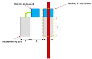
POC filter designing by selecting TDK network8.

The application requires L2 and R2 to be connected to the RIN+ line simultaneously.

I would like to inquire about the routing guide accordingly.

  • Hello, 

    Due to US public holiday on Friday 4/18/25, support will resume on Monday. Thank you for your patience. 

    Regards, 

    Logan

  • Hello Hyeok,

    For the PoC inductor, we typically aim to have a single continuous pad touching the high-speed RIN+/DOUT+ trace. Then, anti-pads would be added such that impedance mismatch is controlled at the PoC inductor landing pad.

    In this case, you should place the L2 and R2 landing pads as close as possible, such that there is a continuous single pad being formed, when touching the RIN+/DOUT+ trace. And then add an anti-pad accordingly. Below is a general approximation.


    Please also make sure you are referring to the FPD3 Channel Specs (Rev 0.8.1) when designing your system with the 954 chip. And verify you are meeting the IL/RL targets in your own system.

    I am not sure how large your PCB is, but please keep in mind that these components may make routing of the RIN+/DOUT+ traces a bit difficult.

    Best,

    Justin Phan