Other Parts Discussed in Thread: TMUX1511, SN74CBTLV3126, SN74LV125A
Tool/software:
Hi, Sir,
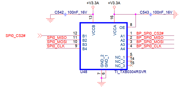
We have a motherboard (CPU: Intel Core i5-1335UE) that uses the TXB0304RSVR as a level shifter to convert SPI from 3.3V standby power (3.3VSB) to SPI 3.3V main power (3.3VCC).
However, we’ve encountered an issue with this configuration.
Schematic:
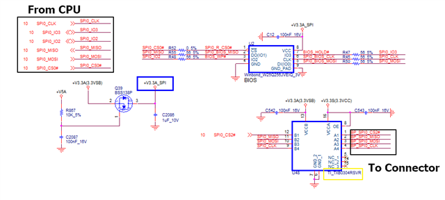
When the ATX power pulls PSON# low to turn on the system, the TXB0304RSVR's OE pin is high, which causes interference to the SPI source (3.3VSB). As a result, the BIOS flash is affected and the system fails to boot.
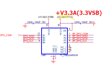
In our experiment, if we connect both the VCCA and OE pins to 3.3VSB (Circuit shown below), the system is able to boot normally.
(Note: During the failure, the connector had no device attached — meaning the A-side SPI lines are floating.)
Questions:
- Is it appropriate to use the TXB0304RSVR for translating SPI from 3.3V standby power (3.3VSB) to SPI 3.3V main power (3.3VCC)?
- Does the above schematic (first schematic) have any design issues?
- Since this is a same-voltage translation, which side (A or B) is recommended to be connected to the SPI source? (In our current design, the source is connected to the B-side.)
Thank you for your support.