This thread has been locked.

If you have a related question, please click the "Ask a related question" button in the top right corner. The newly created question will be automatically linked to this question.

SN75C1167: About the differences in the driver's protection circuit design between the two fabs

Part Number: SN75C1167

Tool/software:

Hi all,

I have a question about the driver specifications of SN75C1167 related to PCN# 20240221006.1.

When a customer performed an in-circuit test (ICT), the following differences were found between SHE and RFAB products.

Voltage value of driver pins (pins 13 and 14):

 SHE product: 0.5V
 RFB product: 1.2V (OL displayed)

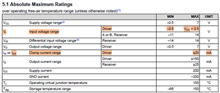
According to the following datasheet, these pins have ESD diodes implemented on both Vcc and GND.

If Vcc = 0V and DE of pin 12 is 0V, the voltage that would turn on the driver's ESD diode would be around +/-0.5V according to the datasheet specifications.

Is there a difference in the design of the driver's protection circuit between the two fabs?

Best regards,
Toshi

  • The driver input pins are 1D/2D (9/15).

    The driver output pins might have clamps to GND, but not to VCC. Your measurements show that the RFB die does not have diode clamps to GND, so I guess ESD protection is implemented in another way.

  • Hi Toshi,

    I believe the Sherman Fab used older process technology from the 90s which were mostly BJT based. The newer process technology made from RFAB are CMOS. The designs between the two of them are not the same for this reason. (You can't copy paste the design from old to new process technology). So you may see differences in ICT for newer dies.

    -Bobby

  • Clement-san,
     Thank you for pointing out the Driver IN specifications.

    Bobby-san, 
    I understand that the RFAB DIE has been completely redesigned.
    I have questions about this.

    The Io(off) specifications are as follows.

        When Vcc=0V & Vo=6V, Io(off)=+100uA(max)
        When Vcc=0V & Vo=-0.25V, Io(off)=-100uA(Max)


    Is it correct that this means that HiZ is maintained up to Vo=6V?
    Furthermore, since the RFAB DIE is CMOS, does this mean that this value may be smaller than Sherman DIE?

    The absolute maximum rating of Driver Vo is -0.5V to 7V.
    Iok is +/-20mA.
    Is the Driver clamp voltage -0.5V and 7V?

    Thank you in advance.
    Best regards,
    Toshi

  • Is it correct that this means that HiZ is maintained up to Vo=6V?

    Yes, this is how I interpret this spec as well. I believe if the device is unpowered and you pull the voltage above 6V, you will see the current spike due to diodes beginning to conduct. 

    Furthermore, since the RFAB DIE is CMOS, does this mean that this value may be smaller than Sherman DIE?

    I don't think this is guaranteed to be smaller because this isn't directly related to the transistor value. I believe the conduction/leakage may be coming from a diode/ESD cell instead.

    The absolute maximum rating of Driver Vo is -0.5V to 7V.
    Iok is +/-20mA.
    Is the Driver clamp voltage -0.5V and 7V?

    The absolute max voltages are a system level requirement that the customer needs to ensure. It does not mean our device is clamping the voltage to these values.

    -Bobby