This thread has been locked.

If you have a related question, please click the "Ask a related question" button in the top right corner. The newly created question will be automatically linked to this question.

SN75LVPE5412: SN75LVPE5412, SN75LVPE5421 I2C reigster address

Part Number: SN75LVPE5412
Other Parts Discussed in Thread: SN75LVPE5421

Tool/software:

Hello, Ti support team

I am conducting experiments using the ICs SN75LVPE5412 and SN75LVPE5421, changing the EQ Gain and Flat Gain settings.
Could you please tell me the register addresses used when configuring these two settings via I2C communication?
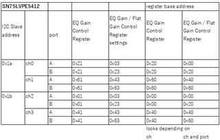
Table 6-5 in the datasheet includes the following information.
Could you explain the differences between addresses 0x00 and 0x20, and between 0x40 and 0x60?
When testing with the actual hardware, it seems that the addresses are used differently depending on whether port A or B is selected, but I couldn't find any mention of this in the datasheet.
If there is any detailed documentation about the Register Base Address, could you please share it with me?

Table 6-5
Channel Registers Base Address
         Channel Bank 0 Access Channel Bank 1 Access
0x00 Channel 0 registers        Channel 2 registers
0x20 Channel 0 registers        Channel 2 registers
0x40 Channel 1 registers        Channel 3 registers
0x60 Channel 1 registers        Channel 3 registers

  • Hi Kunio,

    We have a programming guide covering this device in the Design Resources folder.  Please request access:

    https://www.ti.com/secureresources/PCIE5-REDRIVERS-DESIGN

    This guide has some example register configuration sequences that demonstrate how to configure the device.  Please let us know if you have additional questions.

    Thanks,

    Drew

  • Hi Kunio,

    Your access to the PCIE5-REDRIVERS-DESIGN folder has been approved today. The document Drew is referring to is the "DS320PR412-421 Programming Guide", you may find the programming examples helpful.

    Copied from email, here is the table you provided for "hypothesis based on the results of signal measurements".

    Could you describe in more detail what procedure for signal measurements you used to make your hypothesis? The programming guide is a few years old now and we have been reviewing it to see if any updates or corrections are needed. If you have found behavior that does not match with the datasheet or programming guide descriptions, we will take some time to investigate the matter.

    Best,

    Evan Su

  • Hi Drew and Evan,

    Thank you very much for your response.

    After reviewing the programming guide, there are still a few points that remain unclear to us.

    1. Regarding Register Addresses Based on Port Selection

    As mentioned above, neither Table 6-5 in the document nor the programming guide provides detailed explanations about the register addresses to be accessed. There is also no mention that the register addresses to be configured differ depending on the selected port.

    However, based on our experiments, we have confirmed that the register addresses indeed vary depending on the selected port. Could you please confirm if this observation is correct?

    To verify this, we switched between Port A and Port B, modified the register values for EQ Gain Control / Flat Gain Control via I2C communication, and observed the input and output signal waveforms. We then identified which register changes affected the signal gain.

    The results of this verification are summarized in the table attached by Evan.

    In the programming guide’s sequence, the same values are written to register addresses 0x01 and 0x21. Although the reason for writing identical values is not explained, we assume that these correspond to registers for Port A and Port B respectively.

    2. Regarding the Role of the eq_en_bypass Register

    We would also like to understand the role of the eq_en_bypass register. Our understanding is that setting eq_en_bypass = 0x1 (enable) bypasses eq_stage1.

    However, when we enable eq_en_bypass = 0x1 and change the values of eq_stage1_3:0, we still observe changes in the signal gain. This suggests that eq_stage1 may not actually be bypassed.

    Could you please provide a more detailed explanation of the relationship between the eq_en_bypass register and eq_stage1?

    Thank you for your continued support.

    Best regards,
    Kunio

  • Hi Kunio,

    1. Regarding Register Addresses Based on Port Selection

    As mentioned above, neither Table 6-5 in the document nor the programming guide provides detailed explanations about the register addresses to be accessed. There is also no mention that the register addresses to be configured differ depending on the selected port.

    However, based on our experiments, we have confirmed that the register addresses indeed vary depending on the selected port. Could you please confirm if this observation is correct?

    To verify this, we switched between Port A and Port B, modified the register values for EQ Gain Control / Flat Gain Control via I2C communication, and observed the input and output signal waveforms. We then identified which register changes affected the signal gain.

    Thanks for the information. I will review our documentation and check with our internal teams to clarify what the intended behavior is. Did you perform these hardware tests using the TI DS320PR412-421 EVM or did you use your own board implementing the SN75LVPE5412/421 devices?

    2. Regarding the Role of the eq_en_bypass Register

    We would also like to understand the role of the eq_en_bypass register. Our understanding is that setting eq_en_bypass = 0x1 (enable) bypasses eq_stage1.

    However, when we enable eq_en_bypass = 0x1 and change the values of eq_stage1_3:0, we still observe changes in the signal gain. This suggests that eq_stage1 may not actually be bypassed.

    Could you please provide a more detailed explanation of the relationship between the eq_en_bypass register and eq_stage1?

    The EQ amplifier system is structured like this (diagram from our application note https://www.ti.com/lit/an/snla461/snla461.pdf ):

    "eq_en_bypass" enables or disables the bypass for the "EQ Boost 1 (2nd order)" amplifier (which is controlled by the "eq_profile_3:0" field). But the "EQ Boost 1" amplifier (which is controlled by the "eq_stage1_3:0 field") continues to operate even when the 2nd order is bypassed.

    Best,

    Evan Su

  • Hello Evan,

    Thank you for your reply and your review. I look forward to receiving the results of your internal check.
    > Did you perform these hardware tests using the TI DS320PR412-421 EVM or did you use your own board implementing the SN75LVPE5412/421 devices?
    We use our board implementing the SN75LVPE5412/421 devices.

    Regarding the EQ amplifier system structure. I can understand the structure.
    I would like to confirm just in case :
    Is the following correspondence between the register names and the controlled amplifiers correct?

    Register name : Control amplifier name / function
    eq_stage1 : EQ Boost 1
    eq_stage2 : EQ Boost 2
    eq_profile : EQ Boost 1 (2nd order)
    eq_stage1_bypass : skip "EQ Boost 1 (2nd order)"
    flat_gain : not included in the structure figure.

  • Hi Kunio,

    Is the following correspondence between the register names and the controlled amplifiers correct?

    Register name : Control amplifier name / function
    eq_stage1 : EQ Boost 1
    eq_stage2 : EQ Boost 2
    eq_profile : EQ Boost 1 (2nd order)
    eq_stage1_bypass : skip "EQ Boost 1 (2nd order)"
    flat_gain : not included in the structure figure.

    Yes, this is correct. The flat gain (also known as DC gain) driver is located after the EQ amplifiers.

    Best,

    Evan Su