


Tool/software:
Hello Sir/Ma'am,
Dear TI Support Team,
We are considering using the THVD1451DRBR in our design, where RS-422 signals are routed through a USB Type-C connector with a custom pinout configuration tailored to our application. The pinout mapping is as follows:
| A1 | GND | B12 | GND |
| A2 | NC | B11 | NC |
| A3 | NC | B10 | NC |
| A4 | RS422- A | B9 | VBUS |
| A5 | RS422- B | B8 | NC |
| A6 | RS422- Z | B7 | RS422- Y |
| A7 | RS422- Y | B6 | RS422- Z |
| A8 | NC | B5 | RS422- B |
| A9 | VBUS | B4 | RS422- A |
| A10 | NC | B3 | NC |
| A11 | NC | B2 | NC |
| A12 | GND | B1 | GND |
According to the standard Type C connector pinouts,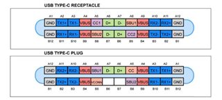
We understand that A4 and B4 are typically assigned to VBUS in the USB Type-C standard. In our design, however, these pins are repurposed to carry RS422-A signals, which connect directly to pin 8 of the THVD1451DRBR.
Our concern is the scenario where a user inadvertently connects a standard USB Type-C power source (e.g., a power brick), which would apply 5V to pin A4/B4. Given that the THVD1451DRBR supports a common-mode voltage range of ±7V, we anticipate that this may not damage the device. However, we would like to confirm:
- Will applying 5V to the RS422-A input (pin 8 of THVD1451DRBR) cause any damage or malfunction?
- If this poses a risk, could you please recommend an alternate IC that can tolerate such a condition or suggest a protection strategy?


