TCAN4550-Q1: How can I know that TCAN4550 are configured well and ready to send CAN message?

Part Number: TCAN4550-Q1
Other Parts Discussed in Thread: TCAN4550,

Tool/software:

Hi Expert,

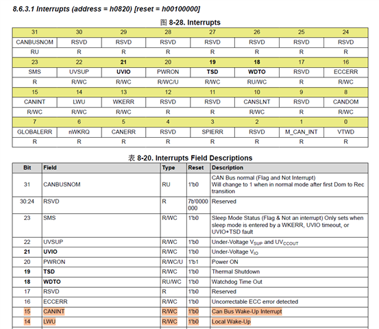
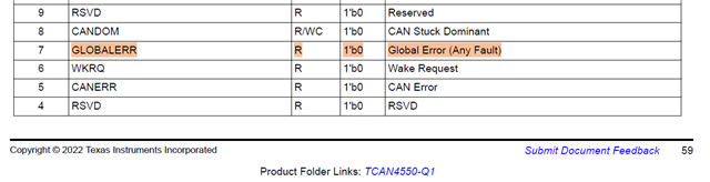
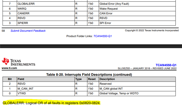
My customers are configuring TCAN4550 software, they wonder if TCAN4550 are configured well and ready to send CAN message, what registers should be read to indicate it, thanks.

Best Regards,

Jack

  • Hi Jack,

    There is not any particular register that will indicate a good configuration.  The customer will need to configure all the MCAN settings such as the nominal and data bit timing, allocate the MRAM space for the number and size of the different RX/TX buffer elements, message ID filters, etc. Once this is done, they will need to transition the device into Normal mode or set the INIT bit in the Control register 0x1018 to 0 to transition the device out of the Initialization Mode and allow it to communicate on the CAN bus.

    Based on the question it sounds like the customer does not have a good understanding of how the device needs to be configured or operates and so I will refer you to some documentation that they need to review.

    TCAN45xx Software User's Guide (Link)

    MCAN User's Manual (Link)

    TCAN455x Clock Optimization and Design Guidelines Application Report (Link)

    Regards,

    Jonathan

  • Hi Jonathan,

    It's observed that there are TCAN4x5x_MCAN_ReadNextFIFO and TCAN4x5x_MCAN_ReadRXBuffer to read RX data in sample code. Could you please tell us more detail differences between the two functions. if we want do more initialization and read the RX data, which one should be used? Thanks.

    Best Regards,

    Jack Li

  • Hi Jack,

    The MCAN controller can be configured to have two RX FIFOs (RX FIFO 0 and RX FIFO 1) and dedicated RX Buffers to store messages.  You do not have to use all of the options, and can configure the device to use only RX FIFO or only dedicated RX Buffers, or a mixture of both RX FIFO and dedicated RX Buffers in combination with different message ID filters to direct the storage of different messages to different locations.

    When using a RX FIFO, you will need to read the RX FIFO Status register to get the buffer number of the FIFO element or elements that contain new messages.  When using dedicated RX Buffers, you will read the New Data registers to see which RX buffers contain new messages.

    The demo code has functions that support both RX FIFO and dedicated RX Buffers.  If you use dedicated RX Buffers, you will need to also setup SID and XID filter elements to direct the storage of new RX messages into the dedicated buffers.  Only the RX FIFOs can be used to accept any RX message without a filter.

    Please review the following documents for more information on RX FIFOs and RX Buffers:

    TCAN45xx Software User's Guide (Link)

    MCAN User's Manual (Link)

    Regards,

    Jonathan

  • Hi Jonathan,

    My customer meet with another problem, please help with it, thanks.

    They could receive correct right data if they just use the receive function, the SPI result is as below:

    However, they receive a wrong data if they use TCAN45550-Q1 to send a data:

    The sending ID is 0x100,sending data is 0x00000100000000

    The received wrong data is 0x215,the data is 0xFFFFFF9F00000000

    Best Regards,

    Jack

  • Hi Jack,

    I'm not really sure what you are trying to show me with the SPI plots, but I do see some potential errors.  The 4th byte transmitted is the "Length" field which is the number of data "words" that will be transmitted or received in this SPI transaction.  Each data word is 4-bytes or 32-bits and this tells the device how many SPI bits and SPI clock cycles it should expect while the Chip Select signal is low.

    A single register read is a total of 64 SPI clock cycles or bits.  The first 32 are from the Header which contains the Read/write Op Code (0x41 or 0x61) followed by the address and the Length byte.  If Length =0x01, then there will be an additional 32 SPI clock cycles or bits transferred while Chip Select is Low.

    If Length = 0x02, then there will be a total of 96 SPI clock cycles (32 from the header, and 64 from the data).

    If Length = 0x03, then there will be a total of 128 SPI clock cycles (32 from the header, and 96 from the data).

    I see in their plots that the chip select stays low for a time period corresponding to Length = 0x01.  Sometimes they correctly set Length = 0x01, and sometimes it is incorrect with 0x02 or 0x08.

    I don't know how they are setting the Length field in their SPI Driver code, but it appears it may have an error and this may or may not be a reason for their other errors.

    Another possible reason is an MRAM allocation error where they have overlapped element times (such as RX FIFO buffer elements with TX Buffer elements causing data to overwrite itself resulting in unexpected data transmission or reception.  I would suggest they also review their MRAM configuration to make sure there are no overlapping elements.

    Regards,

    Jonathan

  • Hi Jonathan,

    Thanks for your kindly response, my customer wonder the way of wake-up, I think we just need wo read the bit14/bit15 of h0820, right?

    Best Regards,

    Jack

  • Jack,

    Yes, to check the source of the wake-up that occurs on the TCAN4550-Q1, the CANINT and LWU bits can be read through SPI.

    Regards,

    Eric Hackett 

  • Hi Eric,

    We notice that the Cwake need to be greater than 10nF in Datasheet, but we just use a 100pF in EVM, is there any wrong?

    Recommend Cwake in Datasheet:

    The EVM schematic is as below:

    Best Regards,

    Jack Li

  • Hi Jack,

    The purpose of the cap is to stabilize the voltage on the pin to avoid false transient switching and false wake events.  A real application in a vehicle is more likely to see this type of transient noise and the EVM is used in a lab environment where this noise is not present.  The EVM board is just an evaluation platform and may or may not have all the components, or components with the required values, that is suitable for all applications.

    The datasheet recommends 10nF for an application.  The datasheet also states that if the WAKE pin is not used that it can be directly connected to either GND or VSUP which would mean that a 10nF cap is not required.  So the customer will need to determine the appropriate value cap and pin configuration for their application.

    Regards,

    Jonathan

  • Hi Jonathan,

    Got it, to save the power, my customer set the VSUP as 6.8V, is there any risk?

    Best Regards,

    Jack Li

  • Hi Jack,

    The only risk is less overhead voltage to the UVLO threshold.  I don't know if they expect any voltage fluctuations from any sort of load dumps, but as long as VSUP remains above the UVLO threshold, then the device should operate normally.

    Regards,

    Jonathan

  • Hi Jonathan,

    What does the GLOBALERR bit means? could you please help to clarify it, thanks.

    Best Regards,

    Jack

  • Hi Jack,

    Please see the note at the bottom of the table.

    This bit is set when any other interrupt bit is set and allows for a single bit to be monitored as an indication that one or more other interrupt bits have been set in either register 0x0820 or 0x0824/0x1050.

    Regards,

    Jonathan

  • Hi Jonathan,

    Thanks for your kindly support, my customer could use the TCAN4550 for CAN message transceiver, I wonder if there is any register could indicate that TCAN4550-Q1 has sent the CAN message successfully? Thanks.

    Best Regards,

    Jack

  • Hi Jack,

    Yes, register 0x10D8 is the TX Buffer Add Request Transmission Occurred register and the bit corresponding to the TX Buffer that was used to transmit the message will be set to 1 when the message has been transmitted.

    The TX Event FIFO can also be configured to store transmission events.

    Regards,

    Jonathan