This thread has been locked.

If you have a related question, please click the "Ask a related question" button in the top right corner. The newly created question will be automatically linked to this question.

DP83630 TPI NETWORK CIRCUIT

Other Parts Discussed in Thread: DP83630

Dear sir, please answer

There is Figure 11 (10/100 Mb/s Twisted Pair Interface) in datasheet.

Please, help me to  identify pins of DP83630 in this figure. 

I guess it must be so:

TPRDM - "RD-" - pin 13

TDRDP - "RD+  -pin 14

TPTDM - "TD-"  - pin 16

TPTDP  - TD+ - pin 17

TIA

Vladimir Naumenkov

www.agat.by

  • Vladimir,

    You are absolutely correct.  By way of clarification, the signal names in the figure are acronyms.  For example, TPRDM stands for "Twisted Pair Receive Differential Minus". 

    Please let me know if you have any additional questions. 

    Patrick

    --

    If this resolves your questions, please don't forget to verify answers to your forum questions by using the green "Verify Answer" button.

  • Dear Patrick

    Thank you

    Please, answer

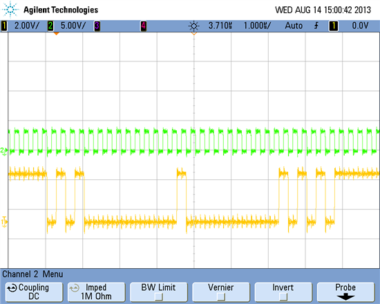
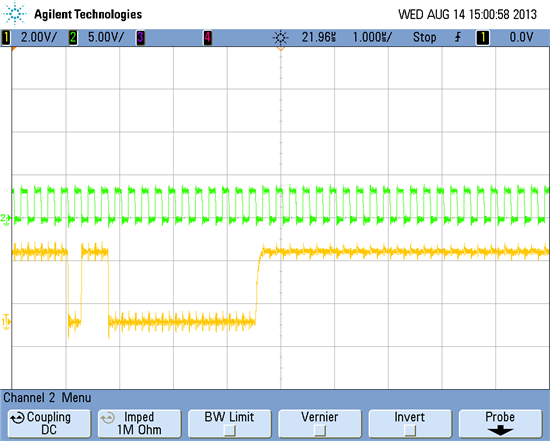
    We are trying to communicate with DP83630 via Serial Management Interface, (we looked  the signals on an oscilloscope) but  the DP83630 still does not respond to requests. We tried to read/write to different registers, but  there is no result. We checked the next: if at the RESET_N and PWRDOWN inputs is "0", then internal generator doesn't work, if at the RESET_N and PWRDOWN inputs is "1", then generator works and we see 25 MHz signals at  X1and X2. Then we checked the next: we strapped pin CLK_OUT_EN  pull-up (pin 21) via 2.2k (сycled power then) and see at CLK_OUT pin, but there is not 25 MHz signal at  this pin. Please, give an advice on what could be done in order to understand whether the DP83630 is OK in principle?  Please, see oscillograms.

    Write REG 0  PHY 0   Data 0x55

    I

    I

    I

    I

    READ REG 0   PHY 0


    TIA

    Sincerely yours

    Vladimir Naumenkov

    www.agat.by

  • Vladimir,

    Your debug approach is thoughtful and well considered.  You are doing the right things in order to understand the issue.

    Regarding the MDIO register access, could you confirm that the Phy Address straps for the Phy agree with the Phy Address in the MDIO sequence?  Are the Phy Address straps set for an address of 0x00? 

    Patrick

  • Dear Patrick

    Thank you

    Yes, the Phy Address straps for the Phy agrees with the Phy Address in the MDIO sequence. We checked again PHY address 0x00 ( that is we strapped PHYAD0 (42 pin) to 0V via 2.2k and other PHY pins has internal pull-down).  We also checked PHY address 0x01 (that is  PHYAD0- PHYAD4 pins has internal strapping only). We also pull-up MDIO pin via 1.5k resistor. 

    We use PIC32 microcontroller (Microchip), it has MIIM interface, which seems to be the same as Serial Management Interface. 

    Please, report: 

    1. If I understand correctly, we can write the data into the register and then read the same data? 

    2.  MDIO pin  first is the input, and at which moment it switches to the output?

    3. I wrote earlier that  we checked the next: we strapped pin CLK_OUT_EN  pull-up (pin 21) via 2.2k (сycled power then) and see at CLK_OUT pin, but there is not 25 MHz signal at  this pin.   QUESTION: to obtain a signal of 25 MHz at  CLK_OUT not required to write any data to the internal  registers via Serial Menagement Interface? It only requires  to strap pin CLK_OUT_EN  pull-up ? 

    TIA

    Yours sincerely

    Vladimir Naumenkov

    www.agat.by

  • Dear Patrick

    Please, answer:

    -can we use "SAU510-USB ISO PLUS JTAG Emulator" with DP83630?

    -whether it is necessary after the power on, to set (for a short time) RESET_N  in "0" ?

    TIA

    Sincerely yours 

    Vladimir Naumenkov

    www.agat.by

  • Vladimir,

    I am not familiar with the JTAG emulator that you mentioned, but the DP83630 is compliant with the 1149.1 specification so I would not anticipate any problems when using a compliant emulator.

    The DP83630 internal circuitry will automatically be reset as part of the power up process.  Note that a reference clock input is required as part of this process.  After power up, it is not necessary to drive the RESET_N pin to 0V as part of the initialization process.

    Patrick

  • Dear Patrick

    Thank you.

    1. Please, specify, you mean reference clock at  X1 input ?

    2. Pin 30 (MDIO): "This pin requires 1.5 k pullup resistor. Alternately, an internal pullup may be enabled by setting  bit 3 in the CDCTRL1 register" . QUESTION: if there is not external pull up resistor, how can we write in CDCTRL1 register - because the Serial Management Interface will not work without this resistor?

    Sincerely yours,

    Vladimir Naumenkov

    www.agat.by

  • Vladimir,

    Yes, I was referring to the reference clock at the X1 Input.  This clock must be running in order to access the registers and in order to generate an output clock.  In terms of device initialization, the timing requirements for X1 during power up and reset are shown in sections 4.5 and 4.6 of the datasheet.

    The MDIO pull up is important for reads from the Phy.  When the Phy is providing read data back to the MAC, the MDIO pin will operate as an open drain output and the MDIO pull up will pull the signal high.  On writes from the MAC, the MAC should be driving the signal so no pull should be necessary.  Therefore, a register write to configure the internal pull up should not pose a problem.

    Note that the internal MDIO pull up is a device specific feature.  This functionality is not described in the IEEE specification.  If the internal pull will be used in a system, it should not be used in systems that share the MDIO interface amongst multiple devices and the functionality should be evaluated carefully during prototyping.

    Patrick