This thread has been locked.

If you have a related question, please click the "Ask a related question" button in the top right corner. The newly created question will be automatically linked to this question.

LMH0071 LVDS Switching Characteristics

Other Parts Discussed in Thread: LMH0071

Hi,

I would like to know if my undertanding is correct about the RX[4:0] Data Valid after/before clock (tDVBC, tDVAC) of LMH0071 Deserializer. In the datasheet the minimum tDVBC and tDVAC is 650 ps, but LMH0071 clock is only 27Mhz or 37 ns. Divide this by 2 due to the DDR clocking and the data period is 18.7 ns. This would make the tDVBC and tDVAC minimum to around 9 ns. Am I right with this?

<Documents>

Datasheet : http://www.ti.com/lit/ds/symlink/lmh0071.pdf

LVDS Timing overview : http://www.ti.com/lit/an/snla122a/snla122a.pdf

Best Regards,

Celmar

  • Hi Celmar,

    This setup/hold time, 650ps, refers to any SDI data rate(270Mbps, 1.485Gbps, and 2.97Gbps). This is the minimum setup and hold time this means in reality it could be longer than 650pS. Having said this, the interface circuit should be able to accept guaranteed  650ps setup and hold time.

    Regards,,nasser

  • Hi Nasser,

    I am only concerned with the minimum RXCLK transition to RX data transistion (tDVAC) wich is 650 ps because in the FPGA side point of view, in case that the tDVAC is 650 ps coming out from LMH0071, the board skew + FPGA internal input skew should not be less than 650 ps between the data and rxclk which is very slim. Although, FPGA can increase the delay of input data with respect rxclk but on the other side the setup time will suffer if the minimum tDVBC coming from LMH0071 is 650 ps.

    I am making a timing constraints for the FPGA input interface, although in reality if tDVBC is on its minimum value the tDVAC should be maximum but it might be tDVAC is on its minimum value and tDVBC is at maximum. So, based on the tDVBC and tDVBC specifaction the worst case timing constraints for FPGA the guaranteed valid time for RX data is tDVBC + tDVAC = 650ps + 650ps = 1.3 ns which is very small for a clock of 27Mhz (37ns). I think that value make sense only at 297Mhz rx clock at 2.97 Gbps data rate and not on 27Mhz rx clock at 270Mps data rate.

    Also, I have observed in the datasheet that the tROCH and tROCL has a minimum of 1.51 ns, the value should only  for 2.97 Gbps capable devices that runs on 297 Mhz clock, and not applicable to LMH0071 because it only runs on 27 Mhz clock. That what makes me doubtful of the minimum 650 ps tDVBC and tDVAC time specification.

    Thank you.


    Regards,

    Celmar

  • Nasser Mohammadi said:

    Hi Celmar,

    This setup/hold time, 650ps, refers to any SDI data rate(270Mbps, 1.485Gbps, and 2.97Gbps). This is the minimum setup and hold time this means in reality it could be longer than 650pS. Having said this, the interface circuit should be able to accept guaranteed  650ps setup and hold time.

    Regards,,nasser

     
    Hi,
     
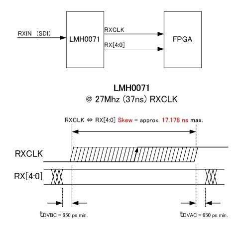
    If that is true, does it mean that the Skew between RXCLK and RX[4:0] is approximately 17.178 ns for an SDI rate of 270 Mbps?  Please see the image below.
    Thank you.
    Regards,
    Celmar
  • Hi Celmar,

    In production every device gets checked to make sure we have at least 650ps  setup or hold time. It means perhaps there could be some devices whereby they have 1200ps setup or 1200ps hold time but we do guarantee on every part data is valid 650ps before or after clock transition. If let's say there is a device that has 650ps setup or hold time then your assumption is correct within the window you have shown the data could be transitioning.

    Regards,,nasser