This thread has been locked.

If you have a related question, please click the "Ask a related question" button in the top right corner. The newly created question will be automatically linked to this question.

SN65HVD3083E input spec

Guru 16770 points
Other Parts Discussed in Thread: SN65HVD3083E

Hi

We want to confirm the input specification for driver.

The following figure is on the datasheet (Figure 4)

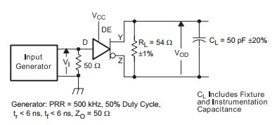
According to this figure, the input is given with 500KHz, 50% duty, tr <6ns, tf <6ns, Zo=50ohm.

For example, should the input meet the tr < 6ns and tf < 6ns when the SN65HVD3083E is used?

BestRegards

  • Figure 4 shows the timings with which some specific tests were made. The timings for which operation is guaranteed can be found in the "Recommended Operation Conditions" table. (Oops. Well, they should be.)

    Anyway, the input is designed to be directly connected to the output of some microcontroller or logic gate.
  • Hi Clemens

    Thank you for your reply.

    If the t_rise and t_fall for input is too slow, it leads to output error, right?

    I'm just wondering what the typical (or max) t_rise and t_fall value for input is.
    (Maybe, < 6ns would be recommended...)

    Bestregards
  • The 6ns values probably were chosen because they give the best result in that particular test (or because that's the best that the signal generator could do). But this is not necessarily the largest allowed value.

    If the omission was deliberate, arbitrary slow inputs are allowed. But if the values were just forgotten, there is an upper limit, and we just do not know it.

    If you look at the digital inputs of other CMOS chips, you see limits such as 100 ns; you could simply assume that the SN65HVD3083E is no worse …
  • There aren't any special restrictions on the rise time of the inputs to HVD3083E; as Clemens suggested, this is a deliberate omission implying that arbitrarily slow inputs are allowed. The 6-ns value shown in the figure is just a product of the function generator used and is shown just so that the test set-up is well-documented. The only issue with very slow-changing signals would be that they would spend more time near the "transition region" of the logic input (i.e., between the low-level and high-level thresholds), and LVTTL/CMOS inputs tend to dissipate more power when the applied voltage is in this region. The transition would have to be extremely (unreasonably) slow before I would expect any issues related to this to be observable, though.

    Max