Part Number: HD3SS215
Hi,
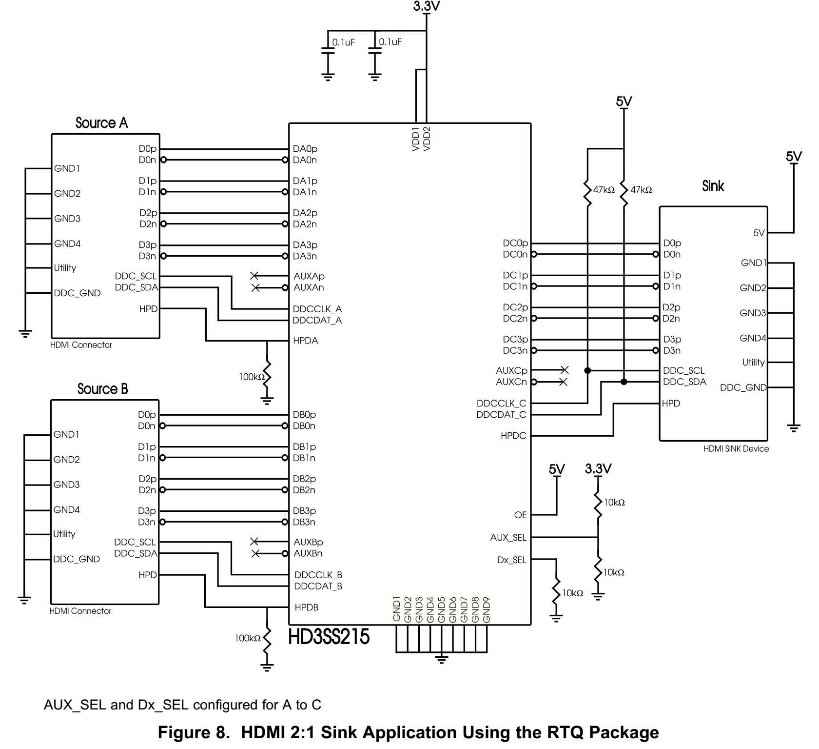
the datasheet for the HD3SS215IZQER states:
9.2.2.2 Detailed Design Procedure
The HD3SS215 is designed to operate with a 3.3 V power supply. Levels above those listed in the Absolute
Ratings table should not be used. If using a higher voltage system power supply, a voltage regulator can be used
to step down to 3.3 V. Decoupling capacitors may be used to reduce noise and improve power supply integrity.
Pull-up resistors to 5 V must be placed on the source side DDC clock and data lines according to the HDMI2.0
Standard. A weak pull down resistor should be placed on the source side HPD line. This is to ensure the source
can differentiate between when HPD is disconnected or at a high voltage level. The AUX_SEL and Dx_SEL
control pins should be set according to the application and desired muxing.
> I understand the pull-up resistors for DDC clock and data need to be placed on the source side with 3V3.
> Fig. 8 shows the pull-up resistors for DDC clock and data one the sink side with 5V.
What is the correct application?
Figure 8