Hi Expert,
We are having a problem when connecting SN75LVDS83A to FPGA.
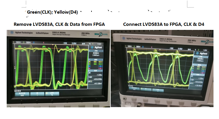
As shown in below capture, if SN75LVDS83A is connected to FPGA with CLKIN & D4. For CLKIN, distortion is found(Green waveform). However, the waveform on D4 pin is normal.
Both CLKIN & D4 are input pin for SN75LVDS83A, why CLKIN signal from FPGA is affected by device, but D4 is not? What is the input structure for CLKIN pin?
Thanks.
Zhou


