This thread has been locked.

If you have a related question, please click the "Ask a related question" button in the top right corner. The newly created question will be automatically linked to this question.

TLK10031: Clock distribution

Part Number: TLK10031

Hi,

We designed a custom board connecting the TLK10031 PHY to a Zync FPGA. We are going to use it in the 10GBASE-SR configuration but currently we don't have any input SFP+ signals (HS) connected. We developed and verified 10G MAC and XAUI on the FPGA but we are not sure about our clock circuit and we don't seem to have the CLKOUT working.

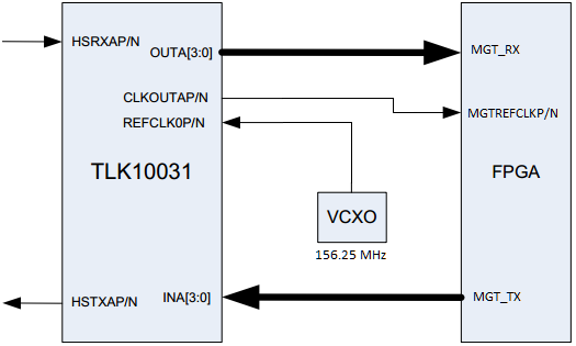
Our clock block diagram is shown below:

This is the block diagram mentioned in the datasheet:

Our questions are:

1. Does our clock connection look correct?

2. We are confused about the block diagram in the datasheet shown in the second image. Does the jitter cleaner outputs the VCXO or the CLKOUT to the FPGA?  Please explain the reference block diagram connection.

3. If our connections are correct, what are the procedures to get CLKOUT to work and test the PHY-FPGA XAUI interface?

4. From our research, we found out that CLKOUT will output half the frequency of the VCXO. So. do we need to use 312.5MHz oscillator instead of 156.25MHz? If needed, we can generate 156.25MHz from an on-chip FPGA PLL and just ignore CLKOUT. So basically PHY is driven by the VCXO and FPGA is driven by another oscillator. Should this configuration work? Do we need any way of synchronization between both PHY and FPGA in this case?

  • Hello,

    We will look into this and get back you as soon as possible.

    Regards,
    Yaser
  • Hello Yaser, thank you for your reply. Will be waiting for your feedback.

  • Hi Yaser, any updates on this?

  • Hi Mohammad,

    Sorry for the late reply. See below for my notes on your questions.

    1. Does our clock connection look correct?

    • Yes the Jitter cleaner is not necessary as long as VCOX is guaranteed to be with the spec listed in the datasheet (i.e. FHSoffset & VID) and have low noise/jitter. See below quote from datasheet section 8.2.2 Detailed Design Procedure.
      • "A differential reference clock must be provided to either the REFCLK0P/N or REFCLK1P/N input port. The clock signal should be AC-coupled and have a differential amplitude between 250 mV and 2000 mV peakto-peak. For 10GBASE-R applications, the clock frequency should be either 156.25 MHz or 312.5 MHz and have an accuracy of 100 ppm. Because jitter on the reference clock can transfer through the TLK10031 PLLs and onto the serial outputs, it is best to keep the reference clock’s jitter as low as possible (that is, under 1 ps from 10 kHz to 20 MHz) in order to meet the requirements of IEEE 802.3."

    2. We are confused about the block diagram in the datasheet shown in the second image. Does the jitter cleaner outputs the VCXO or the CLKOUT to the FPGA?  Please explain the reference block diagram connection.

    • CLKOUT is output to the FPGA. The Jitter cleaner would take in both signals separately and output both separately. 

    3. If our connections are correct, what are the procedures to get CLKOUT to work and test the PHY-FPGA XAUI interface?

    • I would first begin by verifying that the below registers have the expected configuration for your application. Could you describe more what issue you are seeing with CLKOUT? Are you not seeing any output at all?
      • REFCLK_SW_SEL bit field
      • LS_REFCLK_SEL bit field
      • REFCLK_FREQ_SEL_1 bit field
      • REFCLK_FREQ_SEL_0 bit field
      • CLK_CONTROL register

    4. From our research, we found out that CLKOUT will output half the frequency of the VCXO. So. do we need to use 312.5MHz oscillator instead of 156.25MHz? If needed, we can generate 156.25MHz from an on-chip FPGA PLL and just ignore CLKOUT. So basically PHY is driven by the VCXO and FPGA is driven by another oscillator. Should this configuration work? Do we need any way of synchronization between both PHY and FPGA in this case?

    • The recommend configuration is to have CLKOUT connected to FPGA instead of separate PLL. CLKOUT output frequency could change dynamically depending on your system. CLK_CONTROL register the output CLK can be selected to be in the configurations listed in CLKOUT_SEL[3:0] bit field. Also as you mentioned please synchronization between the two clock (if separate) would be needed and can be hard to achieve. 
  • Dear Malik, thank you so much for your answer.

    Our main issue right now is that for the XAUI core (+MDIO controller) inside the FPGA to operate correctly, it requires a 156.25 MHz free running clock. How can we get this clock from the TLK10031 after power up and before sending any MDIO configuration? (because MDIO on the FPGA core needs 156.25MHz clock to operate in the first place!)

  • Mohammad,

    After some digging it seems that you will not be able to get a 156.25 MHz clock output from the CLKOUT pins. Since their is a kind of circular dependency between the FPGA and TLK10031 a 156.25 MHz frequency output is not possible with default setting after power-up in any mode controlled by the MODE_SEL pin. In this case I suggest using a 1 to 2 low jitter clock buffer from the same VCXO.
  • Hello Malik,

    Thanks for your help.

    What about replacing the 156.25MHz oscillator with a 312.5MHz? Then configure the PHY to output 312.5MHz divided by 2 ? We can implement a standalone MDIO controller on the FPGA to do this if it can solve the issue.

  • Mohammad,

    If you can implement a standalone MDIO controller then CLKOUT_DIV[3:0] can be set to divided by 2 to get a 156.25MHz refernce clock output form CLKOUT pins. Is MGTREFCLK the main reference clock for your FPGA? Do you need this reference clock to operate your MDIO interface from the FPGA? I am making the assumption you only have one FPGA.
  • This sounds great, thanks Malik!

    - Yes MGTREFCLK is the main reference clock for the FPGA connected to PHY's CLKOUT.
    - Yes we need this clock for the reference MDIO used within the 10G MAC. That's why we thought of developing a standalone MDIO controller that runs from another 33.33MHz free running clock to configure the Phy.
    - Yes we only have one FPGA.

    Please let us know if you have any comments or better ideas.
  • Mohammad,

    I am glad I was able to help, I do not have any additional comments at the moment. Please let me know if you run into any issues.
  • Much appreciated Malik, will keep you posted if still any issues.