This thread has been locked.

If you have a related question, please click the "Ask a related question" button in the top right corner. The newly created question will be automatically linked to this question.

SN65HVD1040: Circuit Suggestions

Part Number: SN65HVD1040

Hello, 

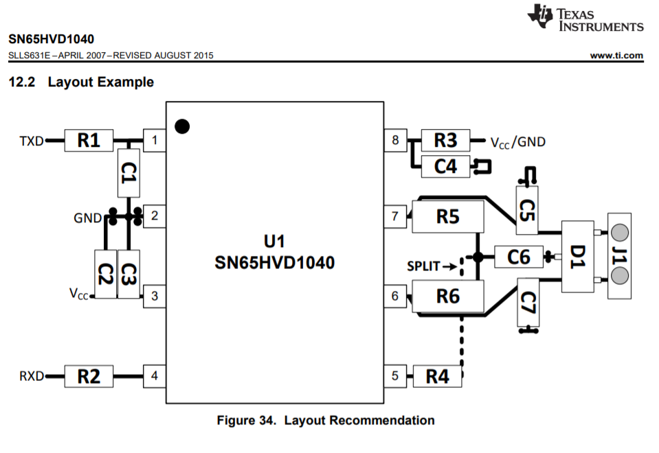
In the d/s's layout recommendation, there is a diagram as below:

1. Could you offer the circuitry to match below layout/

2. What're the recommended values of the R1, R2, C1, C2?

3. Why both C2 and C3 are connected together from below diagram? Is there anything mistake?

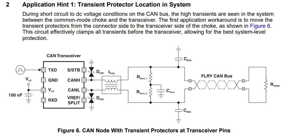
4. I saw some of RS485 circuitry adding a common chock on the output of the RS485 CANH & CANL. What's the purpose?

5. When adding a common chock on the circuit, how to place the TVS? it's located at between RS485 IC and CM chock, correct?

6. Is D1 TVS component?

  • Brian,

    Just to clarify, this is a CAN transceiver, not RS485. I see RS485 mentioned in a few of your questions and I wanted to clarify that before I send my answers.

    1. By circuitry, do you mean schematic of the layout circuit shown?
    2. R1 and R2 can range from 1k to 10k. These resistors are not required, just a precaution to protect the device by limiting any inrush current due to a voltage spike. C1 can be 10pF to 50pF, to help with any high frequency noise, acting as a filter when combined with the resistor. C2 can be a larger bulk capacitance ranging from 5uF to 10uF, and C3 is typically 0.1uF.
    3. Typically with input power to our transceivers, we recommend 0.1uF for high frequency decoupling, and then a larger bulk capacitance to help with other frequencies coming from the power supply but also to help with any voltage dip in the supply voltage. In most systems, this larger bulk capacitance is seen in other parts of the schematic on the power supply line, but it's good to include within the transceiver layout as well.
    4. The choke helps with high frequency noise emitting from the CAN bus, but also filters out high frequency noise from being injected into the CAN bus. It's not necessary for the CAN transceiver to message across the CAN bus correctly, but it helps with signal integrity.
    5. The TVS is typically placed between the choke and the rest of the bus, not between the IC and the choke. Typically it's placed between the termination and the rest of the bus, and the choke is placed between the termination resistor(s) and the IC.
    6. Yes, it is, for the CAN bus.

    Again, this device is a CAN transceiver. Are you looking for RS485 transceivers?

    Regards,

  • Hello Eric,

    I have some questions of using SN65HVD1040 too.

    1. The diagram below is the application of the CM choke. The location of the TVS is between the CAN and CM choke.

        What the differences between this application and your reply beyond? Does it's good to add the 4 TVS at the same time?

    2. If the CM choke is added just for in case, what values of the CM choke is recommended? and the value of the capacitances still be the same as mentioned before? 

    Thank for the reply!

  • Hello Eric,

    I would like to ask some questions:

    1. Does it need to consider the Internal resistance of the PIN1, while designing the value of R1? So does R2?

    2. Does PIN4 need to be designed with a 15pF capacitor as a low pass filter?

    Thanks for the replying!
  • Andy,

    1. What the differences between this application and the reply beyond? Does it's good to to add the 4 TVS diodes at the same time?

    From what I've seen in other applications and what I've read, the main benefit of putting the TVS diodes between the choke and the bus (after all the rest of the passives such as the capacitors) is that the TVS will protect all the components between it and the transceiver from transient voltage spikes. That being said, the components that it would be protecting aren't susceptible to damage from high voltage (in my experience) other than the transceiver. Placing the TVS diodes between the choke and the transceiver may have the benefit to help against kick-back transients from the choke. In general with automotive applications, it's recommended to place the ESD and transient protection diode(s) closest to the connector on the PCB. It's also important to note that though 4 diode symbols are shown, these are actually just two devices on the PCB.

    2. If the CM choke is added just for in case, what values of the CM choke is recommended? and the value of the capacitances still be the same as mentioned before? 

    The capacitances would stay the same, and what I usually see for common-mode choke inductance is 51uH or 100uH.

    3. Does it need to consider the internal resistance of the PIN1, while designing the value of R1? So does R2?

    You should stay within 1k to 3k ohms for R1 and R2, but the lower end of that range is preferred. 1k ohms will be sufficient for the function of those resistors.

    4. Does PIN4 need to be designed with a 15pF capcaitor as a low-pass filter?

    No, this is not a necessary component. It can help with any noise propagating from the bus through the transceiver to the RXD pin, but the device will function fine without it.

    Regards,

  • Hello Eric,

    1. That being said, the components that it would be protecting aren't susceptible to damage from high voltage (in my experience) other than the transceiver.

        It means that in that way only the CAN BUS, CM choke and split node are under the protection, but the transceiver will not be protected? 

        Is there any risk to the transceiver while just adding two TVS between the CM choke and CAN BUS?

    2. If the R1 and R2 are not placed, will the TXD pin be overcurrent?

    Thanks for the replying!

    Best regards!

  • Hello Eric,

    1. The diagram below shows the CAN BUS signal, and both CANH and CANL remains VCC/2 during the Recessive mode.

        How does the CAN IC do this? By internal switches? Is there any structure for helping the comprehension?

    2. If the IC isn't having a SPLIT pin, is it possible to add an external VCC/2 on the middle of the two 60 ohms resistors to reduce the CM noise?

    3. How does 3.5V and 1.5V be obtained?

    4. Under the condition that the transceiver with 3.3V VCC, is the value of CANH and CANL in Recessive mode being 1.65V?

    Thanks a lot for your replying!

  • Hello Eric,
    1. How does the 120 ohms be obtained? From experiences or other methods?
    2. Is the 120 ohms resistor suited for every case? In what case, it may be causing problems?
    Thanks for your patient replying!
  • Andy,

    1. It means that in that way only the CAN BUS, CM choke and split node are under the protection, but the transceiver will not be protected? Is there any risk to the transceiver while just adding two TVS between the CM choke and CAN BUS?

    No, the transceiver will also be protected in this case. The TVS diode will clamp the voltage for every component on the other side of the diodes. The stacked diodes you see in the schematic are actually one packaged component, so the 4 diodes are actually just two components. So no, there is no risk as this is how it is meant to be implemented. If there is going to be TVS diode protection used, then the protection needs to be on both CANH and CANL.

    2. If the R1 and R2 are not placed, ill the TXD pin be overcurrent?

    No, the R1 and R2 are meant to protect from overcurrent in case there is a transient event on the TXD and RXD pins. If they are not there, the pins will still function correctly, but there is risk if a transient is expected on TXD and RXD.

    3. The diagram below shows the CAN BUS signal, and both CANH and CANL remains VCC/2 during the recessive mode. How does the CAN IC do this? By internal switches? Is there any structure for helping the comprehension?

    In the dominant state, two internal switches are enabled to pull CANH up to VCC and CANL down to ground. Once the switches are disabled, the bus recedes to the recessive level through a resistor network biased by VCC. The following diagram illustrates this:

    4. If the IC isn't having a SPLIT pin, is it possible to add an external VCC/2 on the middle of the two 60 ohms resistors to reduce the CM noise?

    It is possible, but not needed. As you said, the SPLIT pin is meant to stabilize the CM voltage to reduce emissions. If there is no SPLIT pin, like on TI's TCAN1042, this means that the device was designed with an even heavier focus on bus symmetry, so that the emissions would be within a desired range without the SPLIT pin. This has been proven through certification testing for automotive, passing without the need for the SPLIT pin.

    5. How does 3.5V and 1.5V be obtained?

    Since there is leakage to the bus due to termination resistance (and other forms of impedance), though the CANH is pulled to VCC and CANL pulled to GND, they won't reach all the way 5V and 0V. The current leaked to the bus will prevent this. This is true for all CAN transceivers.

    6. Under the condition that the transceiver with 3.3V VCC, is the value of CANH and CANL in recessive mode being 1.65V?

    With TI's 3.3V CAN transceivers, it depends. The TCAN33x family of devices has the recessive level at 1.85V. The SN65HVD23x family of devices has the recessive level at 2.3V. The reason for this and trade offs can be found in this post.

    7. How does the 120 ohms be obtained? From experiences or other methods?

    I'm not sure I understand the question. 

    8. Is the 120 ohms resistor suited for every case? In what case it may be causing problems?

    Yes, it is always recommended to use 120 ohms termination at both end nodes on the CAN bus. CAN transceivers are designed to at worst case, to drive 1.5V over 54 ohms effective impedance. The 120 ohm termination resistance is placed at both end nodes to give the bus an effective impedance of 60 ohms.This is necessary for impedance matching of the bus driver, the bus cabling, and the bus receiver. Without the impedance match, you will have reflections of the signal that can corrupt CAN bus messages. High resistances can be placed at the middle nodes on the CAN bus so that there is some damping to help with signal reflections, but the resistances should be high enough that they don't reduce the effective bus resistance to less than 45 ohms.

    Regards,

  • Hello Eric,

    1. I still don't understand that how do the 3.5V and 1.5V be obtained? Is there any structure for helping understanding?

    2. The resistances which values 60 are between the CM choke and CAN BUS.

        How does the function of these 60 ohms ? For making sure that the SPLIT pin being VCC/2?

    3. Why connecting the SPLIT pin can improve the electromagnetic emissions?

    4. If the resistances are designed as 15K ohms and an addition 120 ohms is designed parallel to them(15K ohms) and CAN BUS,  

        how are the effects of the circuit? With advantages or disadvantages?

    5. If the TXD and RXD are connecting the MCU directly, does it necessary to design the buffers between the IC and MCU?

    Thanks for your kind reply !


  • Hello Eric,

    Do you receive my post on 5/27?

    Thanks,

    Best regards!

  • Andy,

    For all of these questions, it would be good to look through this application note. The application note explains the basics of the CAN physical layer.

    1. Internal to the CAN transceiver, there are switches that are enabled to drive the dominant levels on CANH and CANL. These switches pull up to VCC for CANH, and down to GND for CANL. There is also termination resistance and other impedances along the CAN bus which CANH and CANL are connected to, and this creates a leakage path for the current.

    2. These 60 ohm resistors in series add up to 120. This is just another way to create the termination resistance at the end node on the CAN bus.

    3. The SPLIT drives 2.5V to the bus which stabilizes the common-mode level. A lot of emission noise comes from deviations in the common-mode signal, causing a form of switching noise. When the SPLIT pin is driving this level, that deviation and switching noise is lessened because there is a stronger signal driving that common-mode voltage.

    4. Which resistances are you talking about? The termination resistances? 

    5. No, this is not necessary.

    Regards,

  • Hello Eric,

    1. I know CANH will reach to VCC on dominant state. But how is the 3.5V appeared instead of the 5V?Because of the leakage path? Is there any structure for helping understanding?

    2. Yes, if the termination resistance is designed as 30K ohms, what's the difference of effect between the 120 ohms and the 30K ohms?Because most of the suggestion about the value of the termination resistance is 120 ohms, I would like to ask what's the advantage of using 120 ohms? If the 30K ohms is used what's the problems it may lead to?

    Thanks a lot for replying the questions!
  • Andy,

    1. 3.5V (or something less than VCC) is seen instead of 5 because of the drive structure of the transceiver. When the switches are enabled, Rdson will be present, and a voltage drop will occur across this resistance. This happens at both CANH and CANL. This blog illustrates this structure and may make it a bit more clear.

    2. Typical cabling used in CAN applications has a characteristic impedance of 120 ohms. Matching this impedance in your termination resistance will better absorb the signals as they propagate down the CAN bus, and lessen reflections that may cause signal integrity issues. 30k ohms will still help absorb this energy and dampen the reflections, but not near to the level of matching the cable impedance at 120 ohms. The other issue you will see using a higher resistance is your recessive level may not decay down to 2.5V in time for the next bit depending on your data rate. The recessive level isn't "driven" on the CAN bus, the CAN driver "let's go" of the CANH and CANL voltages so that they discharge over the termination resistance and eventually meet at VCC/2. With a 30k ohm termination resistance, this will occur much slower than with 120 ohms, and if your data rate is too fast, the recessive level won't discharge fast enough for the next recessive to dominant edge, and may not meet the threshold of a recessive bit in the receiver circuit.

    Regards,