Because of the holidays, TI E2E™ design support forum responses will be delayed from Dec. 25 through Jan. 2. Thank you for your patience.

This thread has been locked.

If you have a related question, please click the "Ask a related question" button in the top right corner. The newly created question will be automatically linked to this question.

SN65LVELT22: About polarity of output signals

Part Number: SN65LVELT22
Other Parts Discussed in Thread: SN65LVELT23, SN65EPT23, SN65EPT22

Hello support team,

I have some questions about SN65LVELT22 and SN65LVELT23.

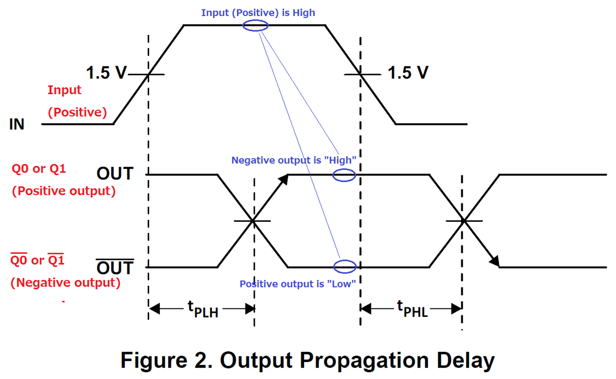
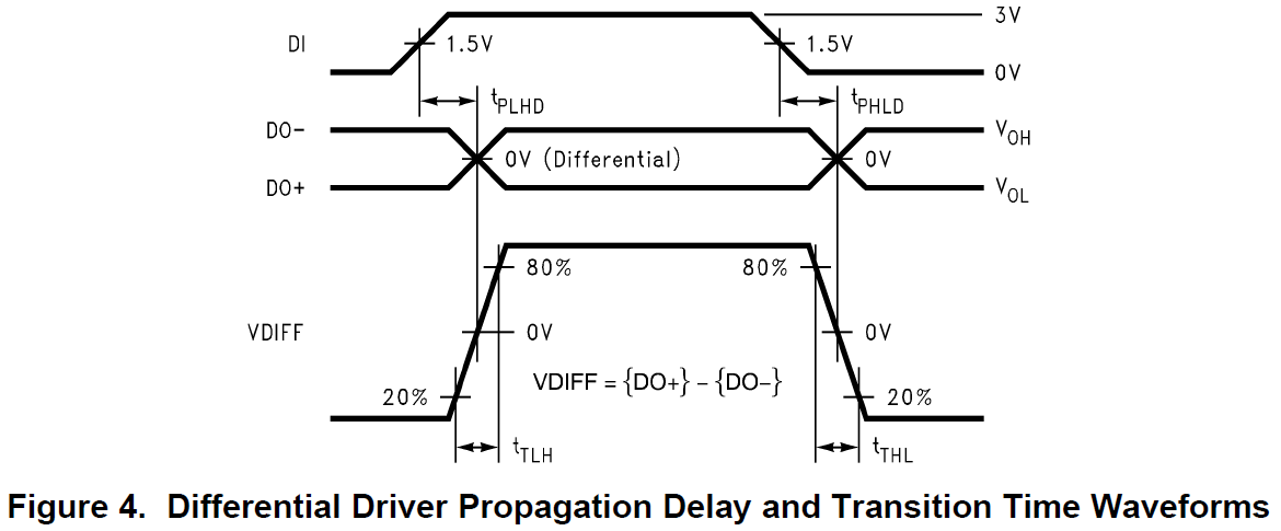
Regarding SN65LVELT22, Figures 2 and 4 on pages 4 and 5 of the datasheet provide time charts for input and output signals.
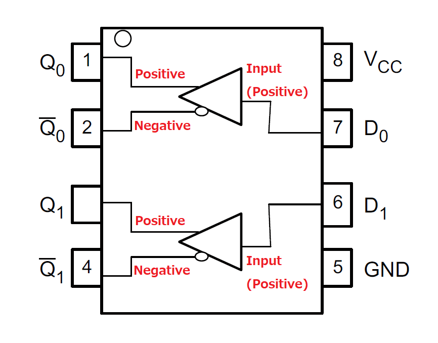
These don't match the signal polarity of block diagram described on page 1 of the datasheet.
Perhaps I think the polarity of the output signals shown in Figure 2 and Figure 4 are reversed.

Also regarding SN65LVELT23, I think the polarity of the output is reversed in Figure 3 of the datasheet.

Is my understanding wrong?

Sincerely,
M. Tachibana

  • Hi Tachibana-san,

    The polarity of the signals are correct on both datasheets. This is what differential signals look like.

    Regards,

    I.K. 

  • Hi Anyiam-san,

    Thank you for your reply.
    I will tell you my thoughts again in detail.

    1) The block diagram explained in "PINOUT ASSIGNMENT" on page 1 of the datasheet of SN65LVELT22 is as follows.

    pin 7 (D0) and pin 6 (D1) are positive inputs.
    pin 1 (Q0) and pin 3? (D1) are positive outputs.
    pin 2 (Q0n) and pin 4 (D1n) are negative outputs.

    2) The description section on page 1 of the data sheet includes the following.
    "The output is driven default high when the inputs are left floating or unused. "

    Furthermore, from IIH and IIL of "TTL DC CHARACTERISTICS" on page 3, I infer that the inputs are pulled up.

    From the above 1) and 2),
    if 'High' signals are input to pin 7 (D0) and pin 6 (D1), the positive output of pin 1 (Q0) and pin 3? (D1) should output 'High' signals.
    And the negative output of pin 2 (Q0n) and pin 4 (D1n) should output 'Low' signals.

    Is my understanding so far wrong?


    On the other hand,
    in Figure 2 on page 4, when 'High' signals are input to pin 7 (D0) and pin 6 (D1), the positive outputs of pin 1 (Q0) and pin 3? (D1) are 'Low', and the negative outputs of pin 2 (Q0n) and pin 4 (D1n) are 'High'.

     So, I suspect that the polarity of Figure 2 is inverted.

    By the way, Figure 4 on page 4 of DS90LV01 datasheet is as my understanding.

    Could you comment again?

    Sincerely,
    M. Tachibana

  • Hi Tachibana-san,

    My mistake, I believe you are correct. It should look like the figure in the DS90LV01 datasheet. It looks like the SN65LVELT22 and SN65LVELT23 datasheets have typos. Thank you for bringing this to our attention.

    Regards,

    I.K. 

  • Hi Anyiam-san,

    Thank you for checking.
    I understood.
    I think SN65EPT22 and SN65EPT23 etc. are wrong as well.

    I appreciate your prompt response.

    Sincerely,
    M. Tachibana