Because of the Thanksgiving holiday in the U.S., TI E2E™ design support forum responses may be delayed from November 25 through December 2. Thank you for your patience.

This thread has been locked.

If you have a related question, please click the "Ask a related question" button in the top right corner. The newly created question will be automatically linked to this question.

SN75157: Differential Line Receiver electrical characteristics and interface MCU

Part Number: SN75157
Other Parts Discussed in Thread: AM26LS31

Hello

I have a question in a block diagram.

Please may I explain in detail.

Q1> Are there any problems with UART connection due to the differential line receiver (SN75157) interface and electrical characteristics in [Fig 2]?

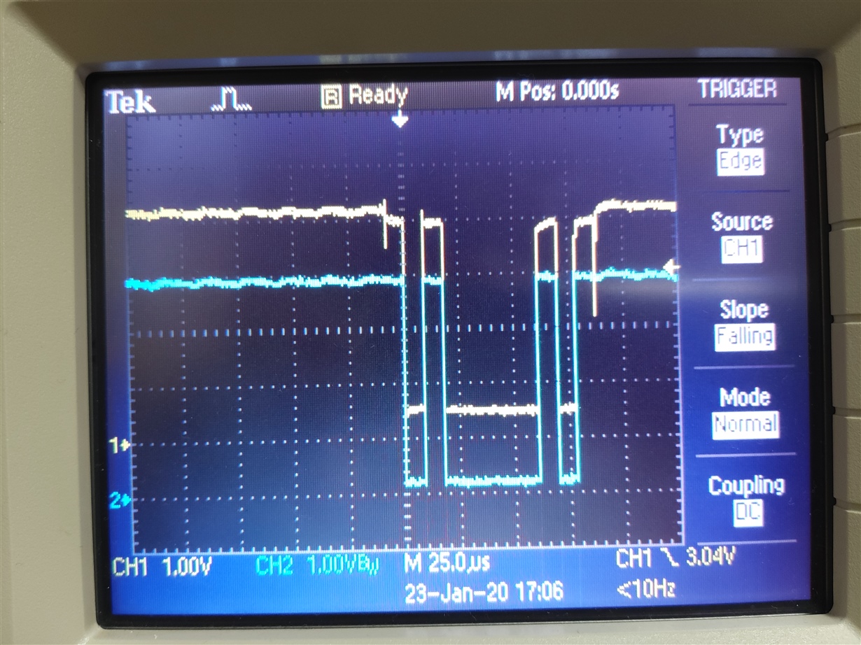
Q2> [Fig 4] is output signal of Differential Line Receiver (AM26LS32ACPW) IC of [Fig 1].

       Sometimes the reference potential starts from above. Or the reference potential starts from below.

      I don't know why. Is this the problem with the device (AM26LS32ACPW)?

Q2-1> Also, Is there a problem with the differential line receiver (SN75157)?

Q3> Is there any problem with the resistance value of Rt 120ohm and the electrical characteristics of the slave in [Fig 2]?

Q4> Are the output waveforms of the SN75157 input signals IN + (A-out) and IN- (A + out) in [Fig 2] correct?

Best Regards,

Jame,Shin

  • Hi Jame,

    Q1> Are there any problems with UART connection due to the differential line receiver (SN75157) interface and electrical characteristics in [Fig 2]?

    I don’t see any issue with these connections. The digital outputs on SN75157 are 3.5V typical for Voh and should be compatible with 3.3V digital signals assuming the receiving device can tolerate these levels. Note that this typical value is under load and the maximum output may be closer to Vcc.

    Q2> [Fig 4] is output signal of Differential Line Receiver (AM26LS32ACPW) IC of [Fig 1].

    Like many RS-422/485 receivers, the output state will be indeterminate when the input Vid is floating somewhere between thresholds Vit- and Vit+. A common method of dealing with this state is by adding a fail-safe biasing network to the RS-422 lines so they remain in a valid state when not actively driven.

    Q3> Is there any problem with the resistance value of Rt 120ohm and the electrical characteristics of the slave in [Fig 2]?

    Termination resistances should be selected to match the impedance of the cable being used to dampen signal reflections. It is recommended that this is done at all end-nodes. In your diagram, is there termination also being applied at the slave end to the right in [Fig1]? If termination also exists here, you may risk over-loading the Line Driver with too much load (too little resistance between lines) and it will not be able to pull a valid differential. This may only become an issue with more termination and can be accommodated for by increasing the resistor values, though this is less ideal for reflection dampening.

    Q4> Are the output waveforms of the SN75157 input signals IN + (A-out) and IN- (A + out) in [Fig 2] correct?

    Ch3 and Ch4 look like typical RS-422 signals. SN75157 should have no trouble translating these to their digital equivalents. The receiver only has one output per channel. Where are A+in and A-in (Ch1 and Ch2) being measured from relative to SN75157?

    I hope this helps. Let me know if everything makes sense or if you have any more questions. 

    Regards,

    Eric


  • Hello Eric

    Thank you for the answer.

    Eric said> I don’t see any issue with these connections.

    Q5> Is the SN75157 output waveform in [Fig 2] the same as the input waveform reference to (IN +) 1 pin among the input signals IN + and IN-?

           i.e.) Like the waveform in [Fig 2], is the output logic swing from high to low with IN + _1Pin (Aout of Ch4 [Fig3] )  &  IN-_7Pin (A + out of Ch3 [Fig3] ) inputs?

                 Important to me, Please may I explain in detail.

    Eric said> The digital outputs on SN75157 are 3.5V typical for Voh and should be compatible with 3.3V ……   tolerate these levels.

             A> The input voltage of TiVa MCU is Vih: (min) 0.65 * VDD = 2.145V (max) 5.5V / Vil: (min) 0V (max) 0.35 * VDD = 1.155V tolerate.

                  The 3.3V pullup resistor 10K is the SN75157 output applied in preparation for floating.

                  In addition, pullup means that the interrupt is generated when the Rx pin of the UART goes Low.

                 Therefore, the 3.5V output voltage is compatible with the input voltage of the MCU.

    Eric said> It is recommended that this is done at all end-nodes. 

                    In your diagram, is there termination also being applied at the slave end to the right in [Fig1]?

          Q6> Do both ends of the master and slave require an Rt resistor and do not need Rt between the both ends of the SN75157's input signal?

                  (I'm not sure if there is a slave Rt resistor, I probably applied.)

                 As a countermeasure against the circuit, I am worried about whether Rt should be prepared between both ends of SN75157's input signal.

    Eric said> If termination also exists here, you may risk over-loading the Line Driver with too much load (too little resistance between lines)

                  and it will not be able to pull a valid differential.

           Q7> Why is the theory because the resistance between the lines is small and the current is consumed by the overload?

                  (e.g.   1 / Rt = 1 / Rt (node1) + 1 / Rt (node2) +… .., I = V / Rt so the resistance is small?)

    Eric said> Ch3 and Ch4 look like typical RS-422 signals. SN75157 should have no trouble translating these to their digital equivalents.

           Q8>  “translating these to their digital equivalents. “I didn't understand this.

    Eric said> The receiver only has one output per channel. Where are A+in and A-in (Ch1 and Ch2) being measured from relative to SN75157?

            A> A + in and A-in (Ch1 and Ch2) scope waveforms are AM26LS32ACPW device inputs, i.e.) master output waveforms.

                  (The reduced waveform is due to the Rt resistance.)

    Best Regards,

    Jame,Shin

  • Hi Jame,

    Q5> Is the SN75157 output waveform in [Fig 2] the same as the input waveform reference to (IN +) 1 pin

    Yes. If (IN-) is held at a constant potential, the receiver (OUT) will follow the state of (IN+) as long as the input magnitude is outside the indeterminate input zone. This is demonstrated in the Test Circuit in Figure 1 of the datasheet. Please refer to the table for typical Differential Line Receiver output states

    Differential Input

    Output

    ID­ = (IN+) – (IN-)

    R

    ID­ > VIT+

    HIGH

    ID­ < VIT-

    LOW

    VIT- < V­ID­ < VIT+

    ??


    Q6> Do both ends of the master and slave require an Rt resistor

    Termination for RS-422 compliant systems is always placed at the load-end of the cable. Depending on your cable configuration, the SN75157 node may be treated as a stub or daisy chained node without termination. Termination topology will be more dependent on the cable layout than the transceivers used. This application report covers a few suggested termination techniques with benefits and drawbacks: http://www.ti.com/lit/an/slla070d/slla070d.pdf

    Let me know if you have more questions about this. If possible, please include cable lengths, node count, and existing termination placements and values.

    Q7> Why is the theory because the resistance between the lines is small and the current is consumed by the overload?

    In a system with single 120-ohm termination, a RS-422 driver will need to supply enough current to create a valid differential voltage signal across the resistance of the cable. The resulting voltage will be the product of the supplied current and the total resistive loading on the bus (Vdiff = II * RL). If our driver can supply 20mA of current, our resulting Vdiff will be 120ohms * 20mA = 2.4V. After attenuation across the length of the cable, this will likely be adequate to be registered as a valid input outside of receiver indeterminate input range. If we treat the amount of current a driver can supply as relatively fixed, increasing the loading on the bus by adding additional termination (decreasing RL) will decrease the resulting Vdiff generated by the driver. For example, if we add two more 120-ohm terminations to our system, the total loading becomes 40-ohms (three 120s in parallel). If we calculate our resulting Vdiff again we’ll end up with 40ohm * 20mA = 0.8V. This much smaller differential is more likely to be attenuated to through the cable to a value in the receivers’ indeterminate range and communication would fail. Increasing the loading on the bus in this way is what I was referring to as over-loading.

    Q8>  “translating these to their digital equivalents. “I didn't understand this.

    RS-422 receivers convert a differential signal from a bus to a digital signal that can be read by other digital circuitry. The waveforms in the figure above look to be within typical operating conditions for SN75157 and the device should therefore have no issue completing this task.

    A>    A + in and A-in (Ch1 and Ch2) scope waveforms are AM26LS32ACPW device inputs, i.e.) master output waveforms.

    This makes sense. Thank you for sharing.

    Let me know if you would like further clarification on any of these points.

    Regards,

    Eric

  • Hello Eric,

    Thank you for the detailed explanation.

    This question is about the voltage level according to the interface specification.

    EIA-422 (0 V to 5 V swing), MIL-STD-188-114B (0 V centered symmetry), RS422 (-7 V to +7 V swing)

    However, the data sheet describes the electrical properties in the MIL-STD-188-144B specification.

    Q9> “Vid = (IN +) – (IN-) => Output R“ means

           Does it mean that the input voltage difference between the differential lines is output from the receiver?

    Q10> I have analyzed the electrical characteristics of the SN75157 device IC.

           There are questions Q10-1>, Q10-2>, Q10-3> in the picture below.

    Q10-1> Do I need a pull up? When Low from unwanted signal, UART Rx generates INT.

    Q10-2> ?? what do you mean ?. Floating, High, Low ?

    Q10-3> Do you not consider VIT - ?

    <Addition:>

    OUT output of SN75157 device IC should be high when there is no input data.

    Of course, it will depend on the input of the SN75157.

    (i.e.) Output from AM26LS32ACPW (Receiver) and AM26LS31CNSR (Driver) device.

    Q10-4> May I ask you how to make the OUT output (high) state when there is no input data in the SN75157 device ?

    Best Regards,

    Jame,Shin

  • Hello Eric,

    I will wait for your reply.

    Best Regards,

    Jame,Shin

  • Hi Jame,

    Q9> “Vid = (IN +) – (IN-) => Output R“ means. Does it mean that the input voltage difference between the differential lines is output from the receiver?

    The output of the receiver will digitally reflect (output HIGH or LOW) weather the difference between the differential lines is above the positive input threshold (VIT+) or below the negative input threshold (VIT-).

    Q10-2> ?? what do you mean ?. Floating, High, Low ?

    When the difference between the differential lines is between the positive and negative input thresholds, the output of the receiver is indeterminate. This is because the output will depend on the previous state of the input (weather it has more recently crossed the positive or negative threshold). This relationship does not lend itself to state tables. A more accurate representation is depicted in Figure 2 and Figure 3 on the datasheet.


    Q10-3> Do you not consider VIT - ?

    The figure you shared does not seem accurate. Please refer to Figure 2 and Figure 3 on the datasheet for output state relative to differential input state. Let me know if you have any questions about these graphs.

    Q10-1> Do I need a pull up? When Low from unwanted signal, UART Rx generates INT.

    A pull-up resistor will provide a known output in the case that the receiver is un-powered (output pin is HIGH-Z). Because the receiver pin is push-pull, the resistor is not needed while the device is operating normally.

    <Addition:> OUT output of SN75157 device IC should be high when there is no input data.

    Yes, this will depend on the driving state of the bus. In the case where the bus is idle and VID ~= 0.0V (driver output is HIGH-Z), the output of SN75157 will be indeterminate. Because this is undesirable, many system implement a failsafe biasing network to ensure a valid differential exists on the bus when the drivers are in a HIGH-Z state. The previous Application report I shared references this article on Passive Failsafe for Idle Busses: http://www.ti.com/lit/an/slyt324/slyt324.pdf

    Q10-4> May I ask you how to make the OUT output (high) state when there is no input data in the SN75157 device?

    A failsafe biasing network can accomplish this by biasing the bus into a output HIGH state when the AM26LS31CNSR driver is HIGH-Z. This solution only works for a HIGH-Z or shorted bus condition and will not revert to an output HIGH if the bus is actively being driven LOW by AM26LS31CNSR (such as a dominant timeout function). Let me know if you have questions after looking into the linked information on failsafe biasing.

    Regards,

    Eric

  • Hello Eric,

    Thank you for the answer.

    Eric said A10-1> it’s Push-Pull Difference Receiver and Driver Output Circuit. So, Not need Pull Up resistor

    Q11> I understand, I also confirmed (Schematics of input and outputs in DataSheet (SN75157))

    What happens if send the Node-n Driver output while sending data from master to slave in [Figure 3]?

    As a countermeasure to electrical state collision, I think that the driver output should be changed to Open-Collector with floating (3-State) state.

    Please may I explain in detail.

    Eric said A10-2> A more accurate representation is depicted in Figure 2 and Figure 3 on the datasheet.

    Q12> I understand from Figure 2 & 3 in Datasheet . But what is the interpretation of VIC-(Common-mode input voltage) meaning?

           Why do both IN + / IN- input signals enter the SN75157 device IC with the same polarity !! , I do not understand.

    I have read the file(sly324.pdf) you shared with RS-485 Passive failsafe for an idle bus.

    I have seen the final [Figure 3] in the file. Analyze the content by adding modifications to help understanding.

    Q13> Does the VA voltage in the Idle state of the master in [Fig 4] mean that A + out is static high with 2.636V as in the previous post Q10-4> Question?

    Q14> What is the difference between 0.272V and VA-VB voltage difference in [Fig 4]?

             VIT + : means +0.2 V or (VA-VB) – VIT + = 0.272 – 0.2 = 0.072 (Tolerance low margin) !! (i.e.) VID> VIT +: High

    Q15> It is not interpreted whether VA-AB and VAB voltages should be the same or not.

    Best Regards,

    Jame,Shin

  • Hi Jame,

    Q11> What happens if send the Node-n Driver output while sending data from master to slave in [Figure 3]?

    The RS-422 standard does not support this type of functionality. Only one driver may be active on the bus at a time. If this case occurs, it would be considered a fault. Because RS-422 does not define a data layer, it is up to the system designer to ensure this case does not occur.

    As a countermeasure to electrical state collision, I think that the driver output should be changed to Open-Collector with floating (3-State) state.

    When the driver is disabled, the A-B pins become HIGH-Z to allow other nodes to drive the bus. This typically does not occur during a data packet such as to wait for an ACK. In standards such as I2C and CAN, a high impedance state is used to transmit logic high bits which allow multiple devices to drive the data line in quick succession or at the same time. Let me know if this is something you have more questions about.

    Q12> …What is the interpretation of VIC-(Common-mode input voltage) meaning?

    Common-mode Input Voltage refers to the potential at a pin (A-B in this case) with respect to ground. Comparatively, Differential-mode Input Voltage would refer to the voltage between the differential inputs (Vdiff = |VA – VB|). It is recommended that the Common-mode input voltage at these pins does not exceed the value listed on the datasheet as the conditions may cause damage to the device.

    Why do both IN + / IN- input signals enter the SN75157 device IC with the same polarity !

    I don’t think I understand your question. SN75157’s output pin will reflect weather the Differential Input (VID) is above or below a defined threshold (VTH+/-). A valid RS-422 waveform would appear as two data signals that are the inverse of one another. If these two inputs are identical (common mode signal or noise), there should be no change in the device output. This is by design.

    Q13> Does the VA voltage in the Idle state of the master in [Fig 4] mean that A + out is static high with 2.636V as in the previous post Q10-4> Question?

    These calculations look good. The only place I believe there is confusion is the last equation. You have calculated a failsafe differential voltage (VFS) of 0.272V. This means if all nodes have drivers disabled, the bus should rest with this differential between the A and B lines. Because this value is above the RS-422 threshold voltage (VTH+), this will register as a logic HIGH for all receivers on the bus.

    Q14> What is the difference between 0.272V and VA-VB voltage difference in [Fig 4]?

    VFS which you calculated as 0.272V is when all drivers are disabled and the failsafe biasing network is creating the differential on the bus. When a driver is active the equivalent circuit will be different. This will result in a larger differential because a device is sourcing more current than the fail-safe resistors were in the previous case. Let me know if this makes sense or if you would like further clarification.

    VIT + : means +0.2 V or (VA-VB) – VIT + = 0.272 – 0.2 = 0.072 (Tolerance low margin) !! (i.e.) VID> VIT +: High

    As long as differential input VID is greater than the voltage threshold VTH+, the output will be in a known state. In this case, 0.272V > 0.200V so the output is valid HIGH. The output will not toggle until the negative threshold VTH- is reached. This gives an effective noise margin of 0.472V.

    Q15> It is not interpreted whether VA-AB and VAB voltages should be the same or not.

    Differential Input Voltage has many abbreviations. In general: VID = VAB = VA – VB; Vdiff = |VID|

    Regards,

    Eric

  • Hello Eric,

    Thank you for the answer.

    Sorry for many questions.

    Eric_A11> The RS-422 standard does not support this type of functionality. ….. designer to ensure this case does not occur.

    Q16> Which interface is this standard for? Is it RS485? (I do not know RS422 & 485.)

             Or is it I2C (start / stop bit, Salve address, Data, Ack / Nack) or CAN (multi master to Node)?

           The designer needs to define a protocol to avoid problems.

           (e.g.) If the master sends a specific node address that is sent to all nodes, the specific node will be structured to send an ACK signal.

    Eric_A11-1>When the driver is disabled, the A-B pins become HIGH-Z to allow other nodes to drive the bus.

    Q17> [Fig4.] External idle-bus failsafe biasing, VA-VB is 0.272V. And VAB (Vdiff) = 1.26166 V.

             When VIT- <VID <VIT +, HIGH-Z,

           (i.e. -0.2V <VA–VB (0.272V) or VAB (Vdiff) (1.26166V) <+ 0.2V, HIGH-Z condition is not satisfied.)

             Could you please tell me how it becomes HIGH-Z?

    Eric_A11-2> Let me know if this is something you have more questions about.

    Q18> Yes, I'm curious.

    Eric_A12> ….. reflect weather the Differential Input (VID)

    Q19> I understand your answer.

            But,  I'm lack of interpretation for English. “Weather“ I can't translate English well. It means “Status” !!

    Eric_A14> VFS which you calculated as 0.272V … When a driver is active the equivalent circuit will be different.

                 … larger differential because a device is sourcing more current ……

    Q20> VAB (Vdiff) = 1.26166 Is V voltage the voltage that increases as the current increases as you say it?

    Eric_A14_1> This gives an effective noise margin of 0.472V.

    Q21> Is this the sum of 0.272V (VFS) plus negative 0.2V?

    Eric_A15> Differential Input Voltage has many abbreviations.

                 Sorry for not being able to ask clear questions and confused. The contents of Q17 & Q20.

    Best Regards,

    Jame,Shin

  • Hi Jame,

    Q16> Which interface is this [RS-422] standard for?

    RS-422 is another notation for the TIA/EIA-422-B standard. RS-422 and RS-485 are similar industry standard specifications that describe electrical characteristics for differential line drivers and receivers. These devices are commonly used in industrial applications. SN75157 is designed to meet the specifications for the RS-422 standard. This protocol does not allow two transceivers to drive a system bus simultaneously. These standards only specify the physical layer (electrical characteristics) of compliant transceivers and do not define a data layer. The communication format and arbitration methods are often designed to be application specific.  

    Q17> [Fig4.] External idle-bus failsafe biasing, VA-VB is 0.272V. And VAB (Vdiff) = 1.26166 V.

    In this case, 0.272V will be present on the bus when the driver is high-Z. Drivers such as AM26LS31CNSR will have high-impedance outputs when disabled by driving the enable inputs to their in-active state.

    Q18> Yes, I'm curious. [Regarding CAN and I2C]

    CAN (Controller Area Network) and I2C are separate protocols that are often used in automotive and server applications respectively. These protocols use a high-impedance recessive state as logic high and therefore allow multiple drivers to be active at a time. This does not allow both drivers to control the bus, but rather one may overwrite the recessive bus condition of the other by driving dominant. These protocols also define a data layer as well as a physical layer. Because of the ability for drivers to dominant or arbitrate using the bus, the data layer defines how communication should be handled between nodes or devices. For example in CAN, a section of a data packet is used for an arbitration phase allowing important nodes priority to use the bus. 

    Here is some reading material on these two standards:

    CAN: http://www.ti.com/lit/an/sloa101b/sloa101b.pdf

    I2C: http://www.ti.com/lit/sg/sszc003e/sszc003e.pdf

    Let me know if you have specific questions about either of these standards.

    Q19> I understand your answer.

            But,  I'm lack of interpretation for English. “Weather“ I can't translate English well. It means “Status” !!

    Apologies. “...reflect whether the Differential Input (VID)...” English is quite tricky!

    Q20> VAB (Vdiff) = 1.26166 Is V voltage the voltage that increases as the current increases as you say it?

    In your calculations, when the driver is disabled (high-z), the failsafe network will allow the bus to settle to VAB = 0.272V. When the driver is active and driving a logic high (sourcing/sinking current), the bus will reset closer to VAB = 1.26V. 

    Q21> Is this [effective noise margin of 0.472V] the sum of 0.272V (VFS) plus negative 0.2V?

    The distance between VIT- and VFS is what I am referring to. (VFS) - (VIT-) = (0.272V) - (-0.2V) = 4.72V

    Tricky questions are not a problem. I hope you find the information helpful!

    Regards,

    Eric

  • Hello Eric,

    Corrected a previous Post block diagram error. May I you review

    Finally, This question is about the AM26LS32 device IC.

    Q22> Not all 26LS32 device IC output the inverter, but it is not analyzed.

             I don't know if it's an input margin problem or a device IC problem. Why? (Any condition)

    Q23> In [Fig1], is it correct for RS422 to first swing 1B Pin (AIn) ( opposite signal(A+ In, A- In) at the same time )?

             I thought that at the same time the opposite signals were input.

    Best Regards,

    Jame,Shin

  • Hi Jame,

    I do not see much difference between the diagrams apart from the exclusion of pullup resistors on SN75157 output. This is fine. Let me know if you have particular concerns about other parts of the layout.

    Q22> Not all 26LS32 device IC output the inverter, but it is not analyzed.

    All AM26LS32 and other RS-422 compliant differential line receivers should output a logic high when the bus differential is greater than the positive threshold (Dout = HIGH when Va – Vb > Vth+). Inverted logic may occur from mis-wiring the A and B pins. Please check that the probe is attached correctly and that the lines are not switched from driver to receiver.

    Are you able to check the communication on the devices you are testing? Are they able to pass valid data through this system? Inverted logic or flipped polarization would likely cause communication errors to occur.

    Q23> In [Fig1], is it correct for RS422 to first swing 1B Pin (AIn) ( opposite signal(A+ In, A- In) at the same time )?

    This is likely when the line driver switches to an active driving mode from a high impedance standby mode. A logic analyzer may see the B line (A- in) as a high potential when the bus is idle. Once the driver is active, it will pull the bus differential to a logic HIGH state (depending on the digital input). Once activated, we can see the communication continues with several more bits. After this period, it appears the driver goes high impedance again and the A and B lines read the same logic value.

    Let me know if this makes sense.

    Regards,

    Eric

  • Hello Eric,

    Thank you for the answer.

    Sorry for not being able to write short.

    Eric_A20-Q1> Are you able to check the communication on the devices you are testing?

    A> Yes, communication .

         My test environment is as follows:

         The Master and Slave specified in <Block Diagram> in the previous Post were tested with the USB to RS422 Adapter.

         USB to RS422(Master PC)  -> AM26LS32 (Differential Line Receiver) -> AM26LS31(Differential Line Driver) -> RS422 to USB( Slave PC)

    ※ The 26LS32 output generates a suspicious inverter signal as a single end signal,

       but the correct data is displayed in the communication log message window on the slave PC.

    I do not know why the inverter signal is output. Some boards are the same as in the previous post Q22> [Fig4].

    But communication is possible.

    I have no board in question right now.

    Eric_A20-Q2> Are they able to pass valid data through this system?

    A> Yes, I send valid data from Master PC to Salve PC and I receive it without error.

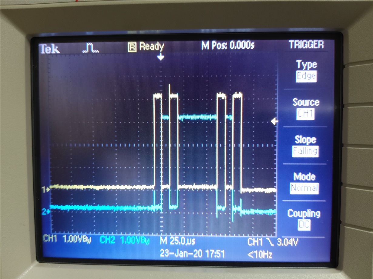
    Q24> In previous Q23, I think the difference between the [Fig1] Master & 26LS32 Connection

             and [Fig2] Master & 26LS32 non-Connection waveform is a hint.

            Looking at the waveform, the A + & A- signals swing in the static High state of [Fig1]

            and swing in the static Low state of [Fig2].

           Why is it, what analysis are you?

    My view is that I am very suspicious of the input / output push pull circuitry of the AM26LS32 device IC.

    Q25> Like this <Block Diagram>, 105 units of P / P produced RS422 interface board.

             Among them, 6 sets of communication test failure occurred.

             I debugged yesterday with similar content that issues the issue.

               The problem board looks like this:

               The A + (1A Pin) / A- (1B Pin) inputs of the AM26LS32 (Differential Line Receiver) are received from

                the USB to RS422 Adapter.

               However, it does not swing only A- (1B Pin) signal but is static high at 5V. ( why 5V ?)

               I have check ESD Protection Diode, Network resister (120 ohm)… connected to the A-input line. ,

               After checking, I replaced the AM26LS32 device IC.

               As a result, the A- (1B Pin) input swings at static high.

               Why did I have this problem? I think a lot.

               Temperature profile in SMT assembly line does not fit, due to ESD,… !!

               I haven't seen it in my workspace. In other spaces, I checked the inverter.

              Think about this. In other spaces, I wonder if it's Power supply ground.

              My doubt is that I / O circuit Push Pull is Vulnerability !!

    Q26> The main point is why the output of the AM26LS32 is why the inverter occurs. Why?

    Best Regards,

    Jame,Shin

  • Hi Jame,

    Q24> Looking at the waveform, the A + & A- signals swing in the static High state of [Fig1] and swing in the static Low state of [Fig2]. Why is it, what analysis are you?

    I believe what you are seeing as a “static high” or “static low” state where both lines are at the same potential. This will occur when the RS-422 driver is disabled and goes high impedance (high-Z). In this state, both A+ and A- lines will decay to the same potential through the 120-ohm termination resistor.

    How are you viewing the state of these lines? Are you using a logic analyzer that only shows you digital state? Would you be able to share images from an oscilloscope? It would be helpful to see what the voltages rest at in each state you describe.

    Q25> Like this <Block Diagram>… 6 sets of communication test failure occurred. The A + (1A Pin) / A- (1B Pin) inputs of the AM26LS32 (Differential Line Receiver) are received from the USB to RS422 Adapter.

    AM26LS32 is only a receiver for RS-422 signals. It appears as a high impedance input on the bus and therefore has very little impact on the bus state. It sounds like you only see one of these lines toggling. Could you ensure your measurement device has a common ground with the RS-422 transmitting device (USB to RS-422)? Not having a common ground may make the readings look like they swing sporadically. If this is not the problem, there may be an issue with the USB to RS-422 device. Since this is what is actually driving the voltages on these lines, failure to do so to RS-422 standards may likely be the result of this device being faulty.

    Could you please share a high-level block diagram of your system including the connected PCs, USB to RS-422 and RS-422 to USB translators and show where in the system you are measuring? If possible, could you share the model of USB to RS-422 device you are using?

    Q26> The main point is why the output of the AM26LS32 is why the inverter occurs. Why?

    Because RS-422 does not define a data layer, it is possible the USB to RS-422 translating device you are using chooses to invert the signal before sending it. This signal is then inverted on the RS-422 to USB receiver device and the slave sees the data with the correct polarity. It is also possible that the slave software auto-detects and corrects the polarity of the incoming signal.

    Regards,

    Eric

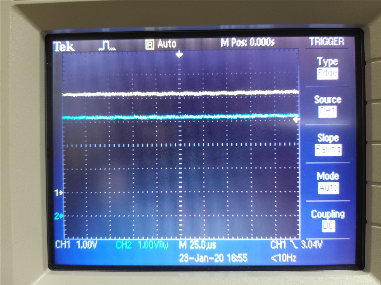
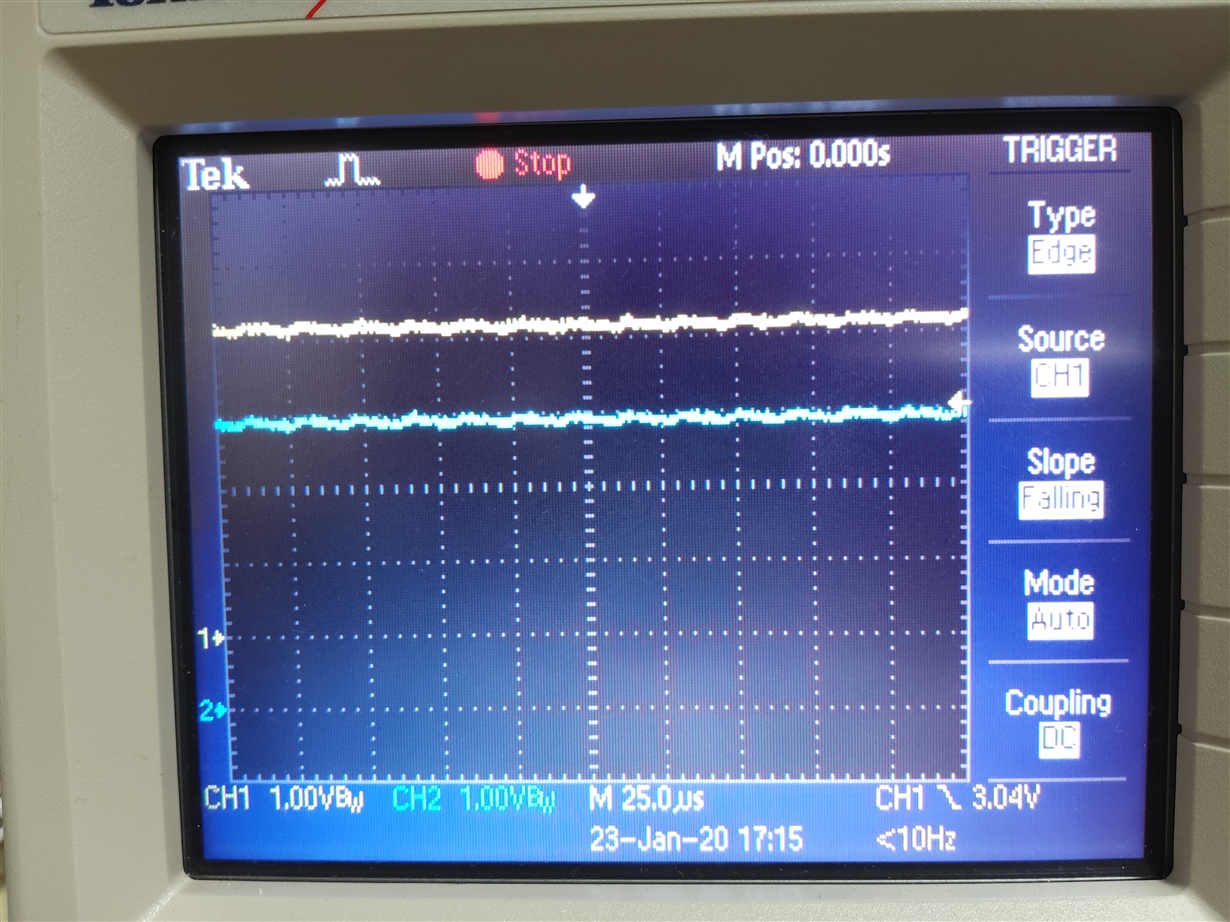
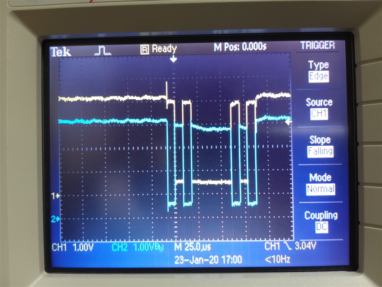
  •                                            [Fig 6.  Ch1: A+ Input,  Ch2: A- (Idle state) ]

                                                        [Fig 7.  Ch1: A+ Input,  Ch2: 26LS32 Output (Idle state) ]


                                                          [Fig 8.  Ch1: A+ Input,  Ch2: A- input (26LS32 Receive State) ]


                                              [Fig 9.  Ch1: A+ Input,  Ch2: 26LS32 Output (26LS32 Output State) ]

          [Fig 10.  Ch1: A+ Input,  Ch2: A- Input (not Connection, Only USB to RS422 Adapter Output  State) ]


    Hello Eric,

    Thank you for the answer.

    Eric_A24-Q1> Are you using a logic analyzer that only shows you digital state?

                  A>   Oscilloscope

    Eric_A25-Q1> Could you ensure your measurement device has a common ground with the RS-422 transmitting device (USB to RS-422)?

                  A>  Yes, See [Fig. 5. USB to RS422],  GND is used in common.

     Eric_A25-Q2> If possible, could you share the model of USB to RS-422 device you are using?

                   A>  Attach the picture and waveform.

                          I'm the same as the one we issued with the previous post.                     

    I know two high impedance occurrences.  

    1. -0.2V  <   (R+) – (R-) ,  i.e. ( Va – Vb) < +0.2V   또는 VIT- ≤ VID ≤ VIT+

            VIT- ≤ VID ≤ VIT+

    2.G Pin (When Low) & Gn Pin (When High) 

    Q27> The R + and R- input voltages are 4.2V when the USB to RS422 Adapter is not connected.        

             It is understood that the output of the 26LS32 outputs either high or low with high impedance.

             i.e.)  R+(4.2V) – R-(4.2V) = 0V

             But I don't know why the output is inverted while receiving data.  below [ Fig 4 ]

              https://e2e.ti.com/support/interface/f/138/p/869375/3228541#3228541

             Can you advise me anything?

    Best Regards,

    Jame,Shin


  • Hi Jame,

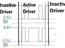
    RS-422 is a differential signal protocol. This means the output of the corresponding bus pins will be inverted from one other to create a differential signal. This is adventitious because it provides signal immunity to ground shifts or common-mode noise. The inverted outputs like in [Fig 4] are deliberate and specified by the standard. Here's a document that outlines the Electrical Specifications for RS-422: RS-422 and RS-485 Standards Overview and System Configurations

    As the original topic of this thread concerns TI's SN75157 being used to interface with an MCU, I would like to ask; are you are still experiencing trouble with this application?

    Regards,

    Eric