Other Parts Discussed in Thread: DS90LV048A, DS92CK16, , SN65LVDS048A, SN65LVDS1, DS90LV027A
Hello,
My customer have noise issue on their production board.
To solve this issue, at first I proposed to boost failsafe function by using external components by following information.
https://www.ti.com/lit/an/snla051c/snla051c.pdf
However, customer had following limitation because they have already released production. So, they can not perform above method at this time.
Here are current their limitation.
* They can NOT change PCB board layout
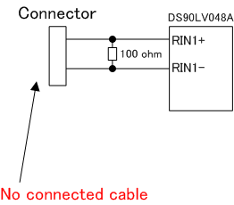
Here is current customer's input for DS90LV048A.
They implemented 100 ohm termination, however there is no cable connection and there is no pattern which can implement PU/PD resistor to boost failsafe function.
It seems that this noise issue is related to differential noise. So, we consider following two things.
1.
Customer asked whether they can perform following method.
* Connect RIN1+ and RIN- to GND
Then I have following question.
Q1. According to datasheet, there is following description in Fail-safe feature.
* Do not tie unused receiver inputs to ground or any other voltages.
It seems that 0V common mode voltage is NOT allowed in this device.
However,on the other hand, there is following description.
"VID is not allowed to be greater than 100 mV when VCM = 0 V or 3 V."
According to above, if VID is less than 100mV, it seems that RIN+ and RIN- can connect GND.
Is there any condition which user can connect RIN1+/RIN- to GND when input is terminated to 100ohm ?
2.
Change to device which have pin compatible and tighter threshold limit(third generation receiver such as DS92CK16).
However, I'm not sure how I can distinglish third generation receiver.
Then I have following question.
Q2. Is there any specific naming rule to understand ?
Best Regards,


