Because of the Thanksgiving holiday in the U.S., TI E2E™ design support forum responses may be delayed from November 25 through December 2. Thank you for your patience.

This thread has been locked.

If you have a related question, please click the "Ask a related question" button in the top right corner. The newly created question will be automatically linked to this question.

TRS213: ESD event causes IC to burn

Expert 1935 points
Part Number: TRS213
Other Parts Discussed in Thread: STRIKE

Hello,

the TRS213 has an integrated ESD protection that works well. But we have one scenario in the field that causes the IC to burn.

The TRS213 is used to level shipft and protect all the pins of a standard serial port. The customer uses the RI pin as 12V supply (POS type application) which under normal cirsumstances does not interfere with the serial port functionality (RX/TX, RTS/CTS are used).

The customer's use case has a powerful 12V/2A power supply attached to RI, so a high current could flow. Far above what a serial port could source.

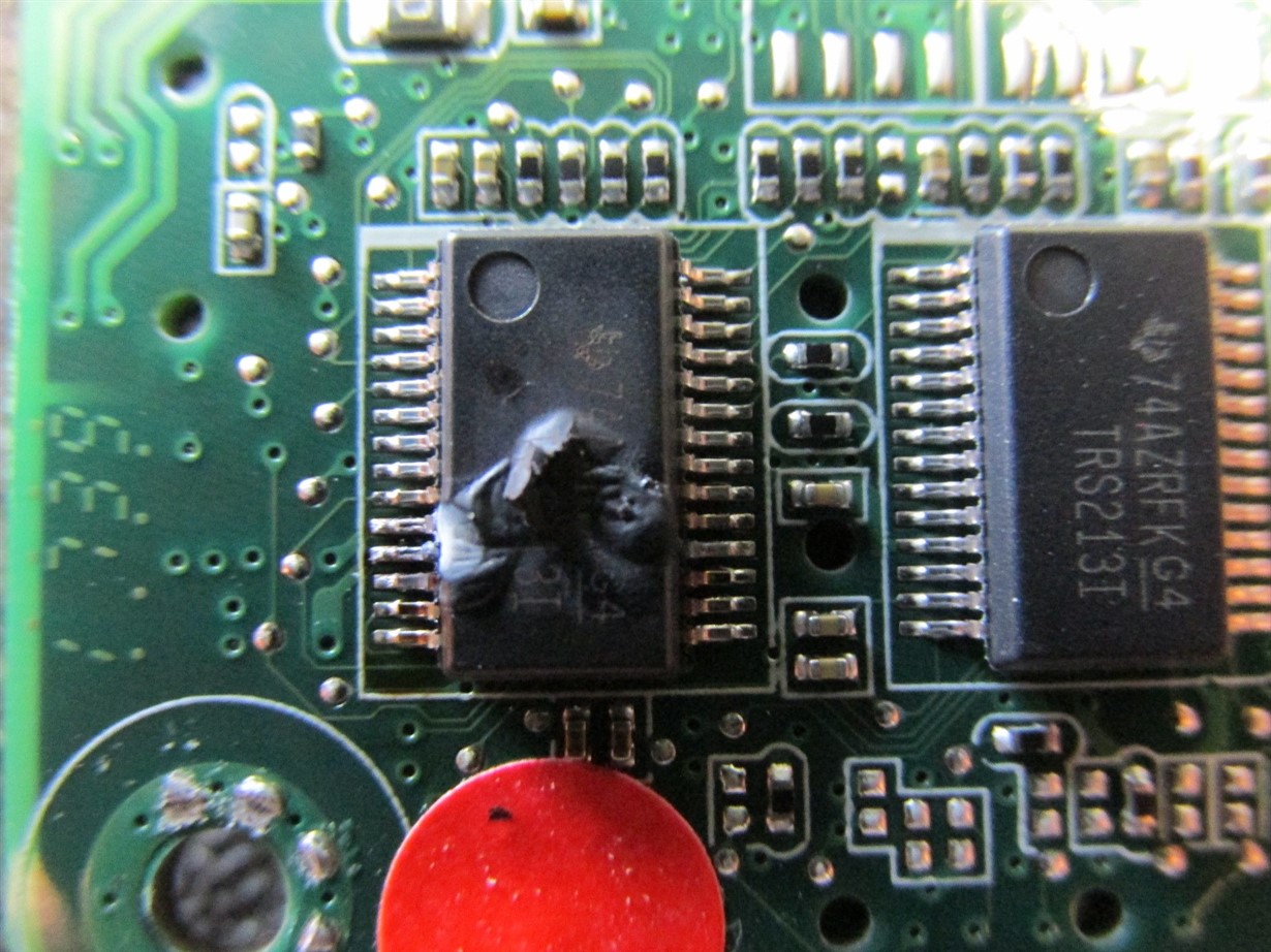
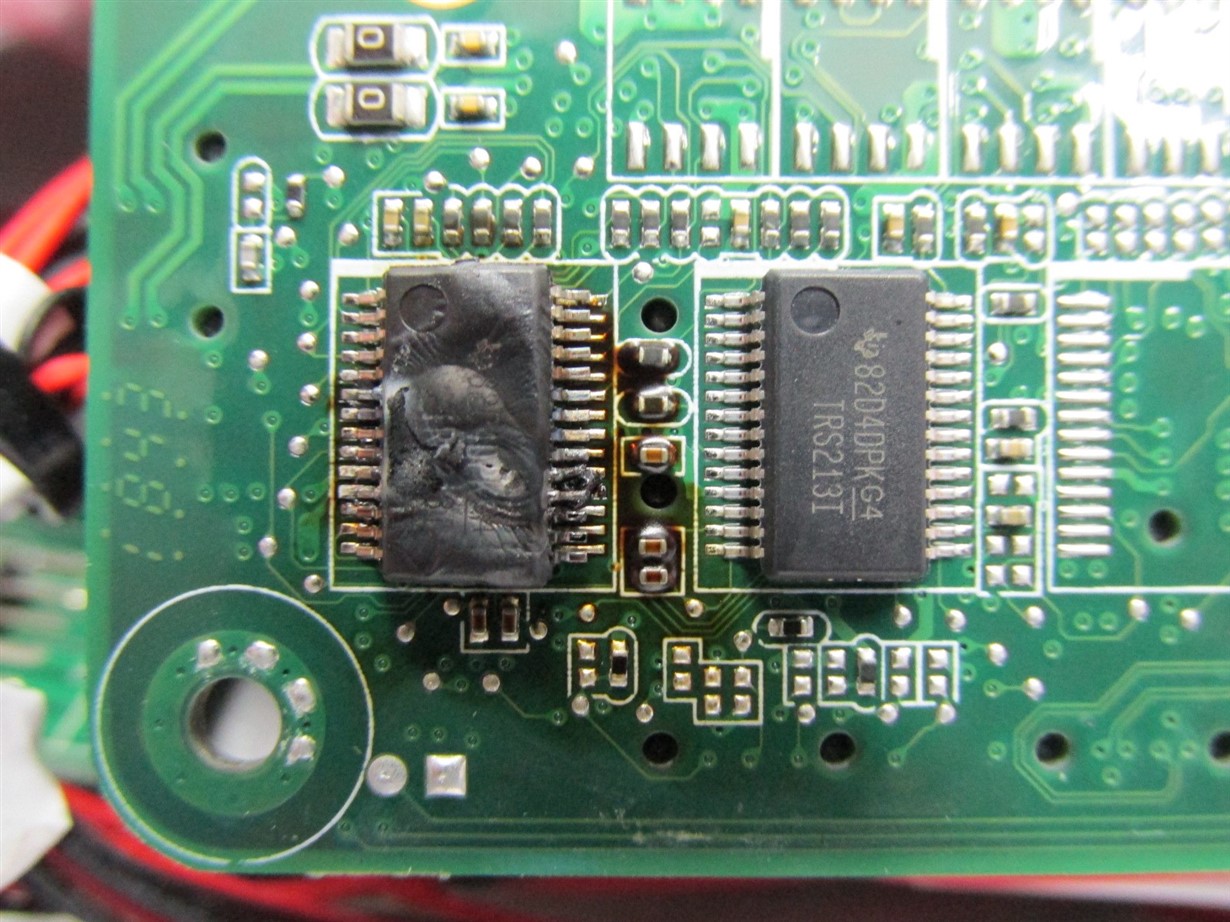
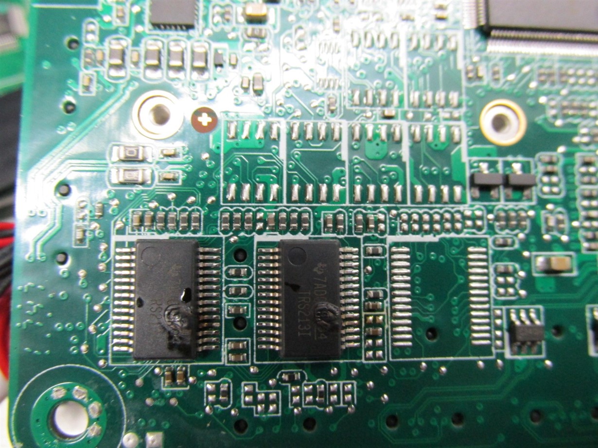
After an ESD event in the lab, when a 12V/2A power supply is attached to RI we can recreate the IC burn up. See pictures below.


In case of an ESD event on the RI pin, I assume that some kind of internal TVS diode starts conducting.

At what voltage would the TVS stop conducting?

Is this voltage current dependent?

Could this scenario explain the result we see?

Best regards,

Lo2

  • Hi Lo2,

    Could you please describe the ESD strike that is applied to the device? If you are following a test standard, please share which one and what level is being tested. Is this a controlled experimental strike or an inadvertent event in the field? 

    The ROUT pins of this device are TTL/CMOS outputs and are not designed to supply power to other devices. Current from this pin will be sourced from Vcc and is not related to the current that is supplied to the corresponding RIN input. 

    The integrated protection circuit in this device will attempt to clamp voltages that exceed the absolute maximum specification each pin. Once conditions return to within this specified range, the protection circuitry will disengage to allow the device to return to normal operation. Please note that these internal circuits are not designed to tolerate or dissipate large amounts of energy. While they may protect from short-lived ESD events, any prolonged DC fault will quickly exceed the heat dissipating capabilities of the circuit and cause permanent damage. 

    Based on your description it seems that the device was internally damage from the ESD event which created some low-impedance path through the device. Once powered by the system, this path allowed a large current to pass through the device, quickly heating and destroying it further. To help address this issue, please share information on the ESD stress being applied to the device is possible. 

    Regards,
    Eric Schott

  • Hi Eric,

    the ESD discharge was generated using a NoiseKen ESS-B3011A ESD Simulator, the voltage was 8kV.

    The following picture shows the tested device, the PCB is inside the case. The TRS213 chips are connected to the three SUB-D9 connectors. The discharge was applied to the indicated locations.

    During this test, the TRS231 behaves as expected.

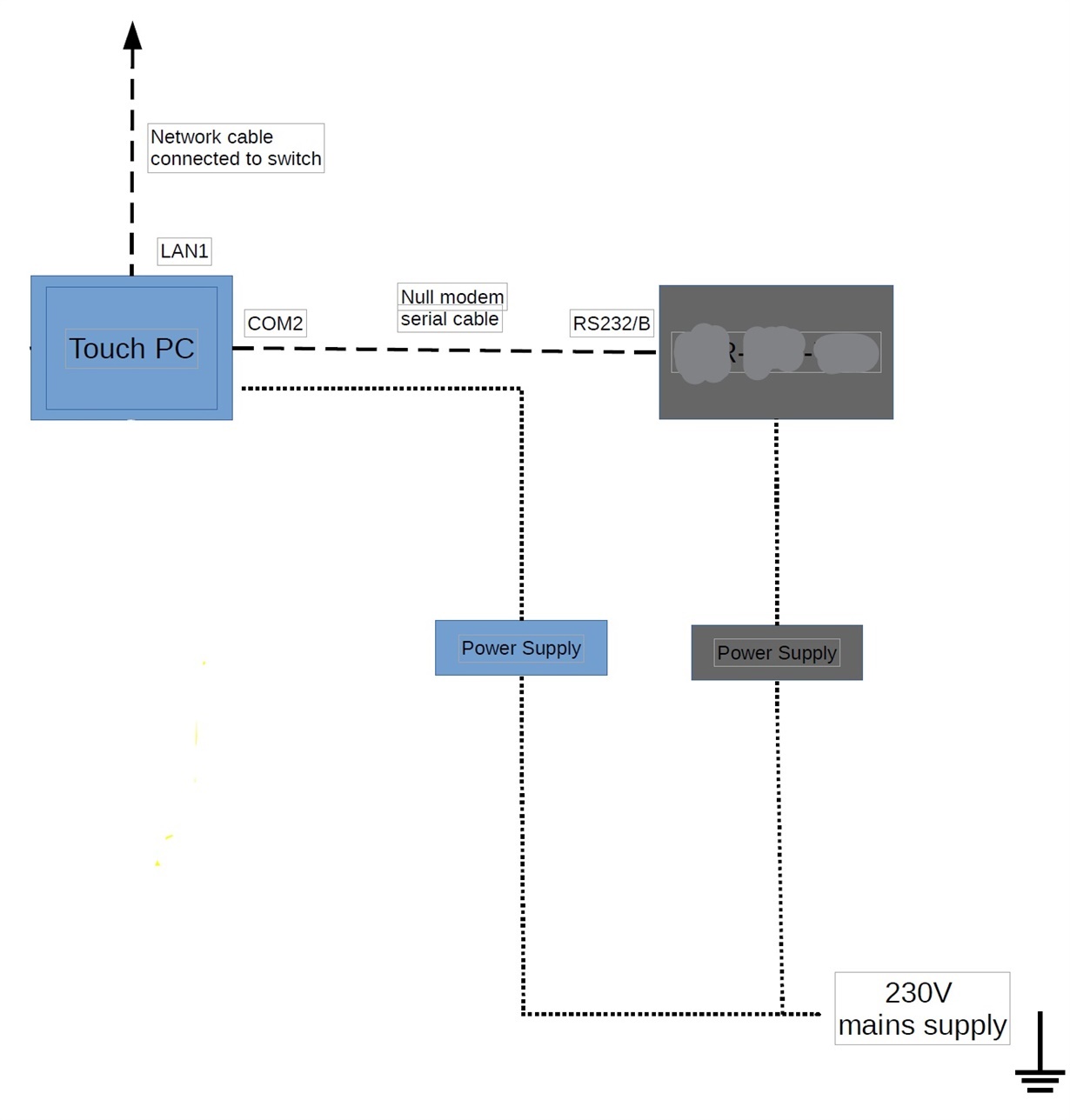
    When the periperhal is attached to COM2 it provides 12V (up to 2A) power to the RI pin of COM2:

    Repeating the same test as shown before causes the IC to burn.

    Our assumption is that the ESD event causes the path to GND to have a low resistance and the 12V/2A keep the TVS diode conductive until it heats up.

    Best regards,

    Lo2

  • Hi Lo2,

    I can't see the images you shared. Can you try uploading them again? You may have to use the "insert image" or "insert file" options. Copy and paste doesn't always work.

  • Hi Eric,

    here are the pictures again:

    Best regards,

    Lo2

  • Lo2,

    Which pin of TRS213 is the RI pin you mentioned? Like Eric said, what ESD standard did you follow? Is it IEC 61000-4-2? TRS213 is rated for 15kV HBM. Another question is if it's possible to measure the RI impedance before and after the strike for comparison.

    Regards,

    Hao

  • Hi Hao,

    the tests were done according IEC 61000-4-2 level3, in this case triggered by an 8kV positive charge.

    This is the pinout of the chip as used on the main board, RI is pin 18:

    The customer kindly measrued the resistance of pin9 on COM1 on a working and a defective unit:

    Equipment used: Fluke 73III
    Setting: black wire to pin 5 of the RS232-Buchse, red write to pin 9
    Measurements

    working device:  4,97 kOhm

    defective device: 47,0 kOhm

    Best regards,

    Lo2

  • Lo2,

    The Rin pins are integrated with 5kOhm pull down resistor internally. The ESD cell placed behind is voltage triggered. Since the abs max is 30V, the triggering point should be higher than it. However the diode doesn't have the capacity to take large current like the other pins. Again TRS213 is not rated at any IEC 61000-4-2 level. The internal circuity could be damaged in different ways by the ESD strike. I suggest you send the failure parts to TI quality team for failure analysis to figure it out.

    Regards,

    Hao

  • Hello Hao,

    thanks for your response!

    I can desolder and send a few of those ICs to TI. I'm located in Europe, should I send them to Freising?

    Feel free to message me or contact me by email.

    Best regards,

    Lo2

  • Lo2,

    You should be able to contact your vendor to reach the TI quality team. The related information can be found on this webpage.

    www.ti.com/.../failure-analysis.html

    Regards,

    Hao