This thread has been locked.

If you have a related question, please click the "Ask a related question" button in the top right corner. The newly created question will be automatically linked to this question.

SN65DSI83: Screen display is unnormal,there is a remnant in gray pattern

Part Number: SN65DSI83
Other Parts Discussed in Thread: DSI-TUNER,

Hi Tis,

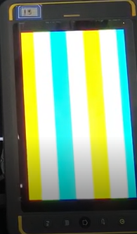
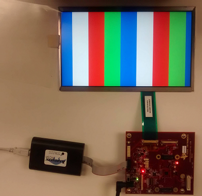
My  Ctm had used the SN65DSI83 as mpi  to lvds bridge.,LCD driver ic is LQ070K1LX80. In gray screen, there is a remnant. 

Would you pls give me some advice?

the code  is as follow:

#define SN65DSI83_BUSNUM 3

static struct i2c_board_info __initdata i2c_sn65dsi83 = { I2C_BOARD_INFO("sn65dsi83", (sn65dsi83_SLAVE_ADDR_WRITE_MOUDLE>>1))};

static int __init sn65dsi83_init(void)
{    
    printk("[sn65dsi83_init] init start\n");
    
    i2c_register_board_info(SN65DSI83_BUSNUM, &i2c_sn65dsi83, 1);

    if(i2c_add_driver(&sn65dsi83_driver)!=0)
    {
        printk("[sn65dsi83_init] failed to register sn65dsi83 i2c driver.\n");
    }
    else
    {
        printk("[sn65dsi83_init] Success to register sn65dsi83 i2c driver.\n");
    }

    return 0;
}

  • Hi Sara,

    1. Are they following the initialization sequence in the datasheet?
    2. Can they share the display datasheet?
    3. Can they use the DSI-Tuner to configure the register settings, and share the .dsi file?

    Regards,
    I.K.
  • Hi,l.K

    The answer is as follows:

    1. Are they following the initialization sequence in the datasheet?

    yes.

    2. Can they share the display datasheet?

    ok,Please see attachment for details.

    3. Can they use the DSI-Tuner to configure the register settings, and share the .dsi file?

    yes,we use the DSI-Tuner to configure the register settings,expect reg 0x12 and 0x19.

    the dsi file please see attachment for details.

    LCD_20180723.rar

  • Hi I.K,

    Thanks for your reply.

    Yes ,CTM use the DSI-Tuner to configure the register setting, the .dsi file refer to the attachment. CTM changed two places, reg 0x12(for mipi clock),reg 0x19 (reducing Snowflake point).

    Display datasheet is  also refer to the attachment.

    Temp.zip

  • Hi Sara,

    1. Can the customer try changing the DE, HSYNC, and VSYNC polarity to positive?
    2. Have they tried the test pattern?
    3. What is the value of register 0xE5 when the issue occurs? (They need to clear this register by writing 0xFF to it before reading from it).
    4. Have they checked the line time (horizontal sync to the next horizontal sync from the processor)? The line time on the input must match the line time on the output (the DSI-Tuner gives the Line Time value in the Outputs window; it's 12.3us) or there will be issues.

    Also, can you expand on your comment about the customer changing registers 0x12 and 0x19? What value did they program these registers? Perhaps provide a register dump?
  • Dear I.K.
    1.CTM use MIPI DSI as their tool, It has those config selection.
    2.Yes,they have tried the test pattern. In test pattern, the screen display is OK.but after quiting the test pattern, there is still a remnant in gray screen.
    3. In the remnant display, register sometimes is 0x0,sometimes is 0x01,if it is right?
    4.CTM has no equipment to measure the mipi signal.
    5.reg 0x12 is 0x24;reg 0x19 is 0x0c.
    Thanks a lot .
  • Sorry, 1.CTM use MIPI DSI as their tool, It has no those config selection.
  • Hi Sara,

    According to the panel datasheet, the polarity of HSYNC, VSYNC, and DE should be positive, do you agree?:

    They should configure it so they're positive polarity. 

    Also, they should not have changed register 0x12 to 0x24. This means they're using a DSI CLK frequency in the range of 180-185MHz. This clock is not fast enough to meet the line time. The DSI CLK needs to be at least 219.9MHz to meet the line time for this application.

    Regards,

    I.K. 

  • Dear I.K.
    Thanks for your reply.
    CTM has set the polarity of HSYNC, VSYNC, and DE to positive and changed reg 0x12 to 0x30. But the remnant still displayed .We have checked the reg 0xE5,the value kept 0x0.
    if there is other regs' could affect the display.
  • Hi Sara,

    If they are able to get the test pattern to display correctly then there is probably something wrong with the DSI side. Have they checked the DSI data lanes for signal integrity issues, and ensured that the electrical/timing specifications are compatible between the SN65DSI83 and their processor?

    They also really need a way to ensure that the line time on the input matches the line time on the output. 

    Regards,
    I.K.

  • Dear I.K,
    CTM has checked their initialization sequence,it is followed the datasheet.So if there are other items that we can check?
    Thanks a lot.
  • Hi Sara,

    They should check the other items I mentioned in my previous post.

    Regards,
    I.K.
  • Hi I.K
    Yes,CTM has checked all the items you mentioned in your previous post. They didn't find any difference.the issue is not solved.So if there are other items that we did not think out? Issue is very urgent. Pls help us kick off the problem. Thanks a lot.
  • Hi Sara,

    Have they checked the line time? They need to ensure it is the same on the DSI side and the LVDS side. Please post a scope screenshot of the line time on the DSI input.

    They also need to check for signal integrity issues on the DSI clock and data lanes. Are these signals clean? Do they meet the electrical/timing specifications in the datasheet?

    Please also provide a register dump when the issue happens.

    As mentioned previously, the fact that they can get the test pattern to display correctly means there's an issue on the DSI side, so they should focus on the above points. How do they enable the test pattern? If they switch from the test pattern to DSI inputs does the issue still appear?

    Regards,
    I.K.
  • Hi I.K

    Thanks for your support.

    Because they don't have test DSI equipment,So we cann't post a scope screenshot of the line time on the DSI input.

    CTM checked their timing sequence ,but found none error.

    the register dump is as follow:

    >>>>>>>dump reg如下:
    
             Line 12027: <0>[ 1470.200782].(1)[3639:sh]----------Reg            write data   read data                  Flag  ==count(46)
             Line 12028: <0>[ 1470.202072].(1)[3639:sh]----------0x9                      0x0                0x0                           0x0 
             Line 12029: <0>[ 1470.203177].(1)[3639:sh]----------0xA                     0x5                0x85               0x1 
             Line 12030: <0>[ 1470.204290].(1)[3639:sh]----------0xB                     0x10              0x10               0x0 
             Line 12032: <0>[ 1470.206615].(1)[3639:sh]----------0x10          0x26              0x26               0x0 
             Line 12033: <0>[ 1470.207750].(1)[3639:sh]----------0x11          0x0                0x0                           0x0 
             Line 12034: <0>[ 1470.208865].(1)[3639:sh]----------0x12          0x30              0x30               0x0 
             Line 12035: <0>[ 1470.210000].(1)[3639:sh]----------0x13          0x0                0x0                           0x0 
             Line 12036: <0>[ 1470.211112].(1)[3639:sh]----------0x18          0x18              0x18               0x0 
             Line 12037: <0>[ 1470.212246].(1)[3639:sh]----------0x19          0xC               0xC                          0x0 
             Line 12038: <0>[ 1470.213359].(1)[3639:sh]----------0x1A                   0x3                0x3                           0x0 
             Line 12039: <0>[ 1470.214471].(1)[3639:sh]----------0x1B                   0x0                0x0                           0x0 
             Line 12040: <0>[ 1470.215636].(1)[3639:sh]----------0x20          0x20              0x20               0x0 
             Line 12042: <0>[ 1470.216822].(1)[3639:sh]----------0x21          0x3                0x3                           0x0 
             Line 12043: <0>[ 1470.217935].(1)[3639:sh]----------0x22          0x0                0x0                           0x0 
             Line 12044: <0>[ 1470.219048].(1)[3639:sh]----------0x23          0x0                0x0                           0x0 
             Line 12045: <0>[ 1470.220160].(1)[3639:sh]----------0x24          0x0                0x0                           0x0 
             Line 12046: <0>[ 1470.221273].(1)[3639:sh]----------0x25          0x0                0x0                           0x0 
             Line 12047: <0>[ 1470.222386].(1)[3639:sh]----------0x26          0x0                0x0                           0x0 
             Line 12048: <0>[ 1470.223499].(1)[3639:sh]----------0x27          0x0                0x0                           0x0 
             Line 12049: <0>[ 1470.224612].(1)[3639:sh]----------0x28          0x21              0x21               0x0 
             Line 12050: <0>[ 1470.225799].(1)[3639:sh]----------0x29          0x0                0x0                           0x0 
             Line 12051: <0>[ 1470.226912].(1)[3639:sh]----------0x2A                   0x0                0x0                           0x0 
             Line 12052: <0>[ 1470.228026].(1)[3639:sh]----------0x2B                   0x0                0x0                           0x0 
             Line 12053: <0>[ 1470.229139].(1)[3639:sh]----------0x2C                   0xA                0xA                          0x0 
             Line 12054: <0>[ 1470.230251].(1)[3639:sh]----------0x2D                   0x0                0x0                           0x0 
             Line 12055: <0>[ 1470.231363].(1)[3639:sh]----------0x2E                   0x0                0x0                           0x0 
             Line 12056: <0>[ 1470.232476].(1)[3639:sh]----------0x2F          0x0                0x0                           0x0 
             Line 12058: <0>[ 1470.233635].(1)[3639:sh]----------0x30          0x8                0x8                           0x0 
             Line 12059: <0>[ 1470.234748].(1)[3639:sh]----------0x31          0x0                0x0                           0x0 
             Line 12060: <0>[ 1470.235976].(1)[3639:sh]----------0x32          0x0                0x0                           0x0 
             Line 12061: <0>[ 1470.237089].(1)[3639:sh]----------0x33          0x0                0x0                           0x0 
             Line 12062: <0>[ 1470.238202].(1)[3639:sh]----------0x34          0x12              0x12               0x0 
             Line 12063: <0>[ 1470.239336].(1)[3639:sh]----------0x35          0x0                0x0                           0x0 
             Line 12064: <0>[ 1470.240448].(1)[3639:sh]----------0x36          0x0                0x0                          0x0 
             Line 12065: <0>[ 1470.241560].(1)[3639:sh]----------0x37          0x0                0x0                           0x0 
             Line 12066: <0>[ 1470.242672].(1)[3639:sh]----------0x38          0x0                0x0                           0x0 
             Line 12067: <0>[ 1470.243784].(1)[3639:sh]----------0x39          0x0                0x0                           0x0 
             Line 12068: <0>[ 1470.245230].(1)[3639:sh]----------0x3A                   0x0                0x0                           0x0 
             Line 12069: <0>[ 1470.246349].(1)[3639:sh]----------0x3B                   0x0                0x0                           0x0 
             Line 12070: <0>[ 1470.247466].(1)[3639:sh]----------0x3C                   0x0                0x0                           0x0 
             Line 12071: <0>[ 1470.248579].(1)[3639:sh]----------0x3D                   0x0                0x0                           0x0 
             Line 12072: <0>[ 1470.249691].(1)[3639:sh]----------0x3E                   0x0                0x0                           0x0 
             Line 12074: <0>[ 1470.250853].(1)[3639:sh]----------0xD                     0x1                0x1                           0x0 
             Line 12075: <0>[ 1470.251955].(1)[3639:sh]----------0x9                      0x1                0x0                           0x1 
             Line 12076: <0>[ 1470.253057].(1)[3639:sh]----------0xFF          0x0                0x0                           0x0
    

    In test pattern,it left a remnant. when we change to active status. we can see it's remnant in gray pattern.

  • Hi Sara,

    It looks like the formatting of the register dump got messed up when you posted it so I am unable to read it. Can you post it as attachment? 

    Also, can you clarify what you mean by "In test pattern, it left a remnant"? Is the test pattern not displaying correctly? Please share an image of it. 

    Regards,

    I.K. 

  • Dear I.K.

    Sorry for saying not clearly, it is displayed correctly in test pattern. After turning off the machine in test pattern,and then turn on and log in normal pattern, we can see it's remnant in gray pattern.the pic as follow:

    Dump Reg.zip

  • Hi Sara,

    Thanks for the update. The remnant of the test pattern is strange. Can you share an image of what the test pattern by itself looks like? It should look like this: e2e.ti.com/.../3348.Untitled.png

    Also, please confirm the below:

    1. Can you share a scope capture showing EN, DA0P, and DACP when EN is asserted? I want to confirm that the initialization sequence is being followed.

    2. Confirm that the DSI clock is continuous (free-running).

    3. Confirm the DSI data lanes are meeting the electrical and timing specifications listed in the datasheet (Table 6.5 and 6.6).

    Regards,
    I.K.
  • Dear I.k

    CTM gave a vedio for test pattern.

    Pls FYI.

    Because  CTM have no test equipment ,so they could not provide  the scope capture. We are checking if local TI office could give hands on this issue.

    Qpad.zip

  • Hi Sara,

    That's not what the test pattern should look like. It should look like this: e2e.ti.com/.../3348.Untitled.png

    Can you share the schematic and layout with me? You can email it to i-anyiam@ti.com if you don't want to share it here.

    Please also keep me updated on the TI office situation as it's very important to have test equipment to help debug the issue.

    Regards,
    I.K.
  • Hi Sara,

    From the schematic, it looks like they have an LDO supply connected to VCORE (pin J8)? VCORE is not an input. It's an output and requires a 1-uF capacitor to GND. Therefore, please cut the trace after C75 and see if that resolves the issue.

    Regards,
    I.K.
  • Dear I.K,
    Thanks for your kindly support.
    The customer has tested your advice, It seems that it resolves their problem,the remnant disappear.The ctm doubted why the plot of Vcore is the same after cut the trace after C75 .
  • Hi Sara,

    The plots may be the same since the LDO output was at the same potential as the VCORE output, 1.1V. After the trace was cut the voltage will still be 1.1V since VCORE is a power supply that outputs 1.1V. VCORE is not an input. It's an output that monitors the internal voltage regulator that is controlled by the EN input, so they should not have an LDO or any other supply connected to this pin.

    Regards,
    I.K.
  • Dear I.K.
    Thanks for your reply. I have told CTM this.
    But CTM checked the method in other devices,the remnant happened again. They explained the reason they didn't find the remnant last Friday,because of short test time. So they think the Vcore is not the reason of remnant.They rectify the Vcore Pin error. If there are other reasons?
  • Hi Sara,

    Does the first device still show the issue? And if they measure Vcore on the other devices, is it at the right voltage level? It's possible the device has been damaged by supplying voltage to this pin.

    What does the test pattern look like after cutting the trace?

    They will need lab equipment to investigate the other possible root causes (line time mismatch and signal integrity issues) I mentioned previously in this thread.

    Regards,
    I.K.
  • Dear I.K.

    Yes, the first device still shows the issue, I have suggested replace the old sn65dsi83 to check if the old one destroyed. the test pattern pic is as follow.

  • Hi Sara,

    It looks like there's some improvement in the test pattern, although it it is still not quite right.

    Previously it looked like this:

    Now it looks like this:

    But if it were correct it should look like this:

    Namely, that gray should be white. 

    So it looks like cutting the trace certainly made a difference. 

    After you replace the unit, please try Joel's suggestion in this thread if the issue persists, as the customer had a very similar looking pattern: https://e2e.ti.com/support/interface/high_speed_interface/f/138/t/486770

    Regards,

    I.K. 

  • Dear I.K,
    CTM measured the VCORE voltage is 1.1V,also replaced SN65dsi83,but the test pattern display was the same as having gray strips.
    Testing advice at the link e2e.ti.com/.../486770,as changing the HSync Pulse Width, has no effect.
  • Hi Sara,

    Please have them check these points in my previous post in a lab: e2e.ti.com/.../2649942

    Also, I can't tell from the files they provided but also make sure they're following layout recommendations: www.ti.com/.../slla340a.pdf

    Regards,
    I.K.