Because of the holidays, TI E2E™ design support forum responses will be delayed from Dec. 25 through Jan. 2. Thank you for your patience.

This thread has been locked.

If you have a related question, please click the "Ask a related question" button in the top right corner. The newly created question will be automatically linked to this question.

LVDS jitter problem using DS90C387A

Other Parts Discussed in Thread: DS90C387A, DS25BR440, DS25BR100

Hi,

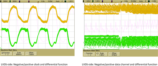
I developed a DVI to LVDS bridge for an optical measurement system. Last week I got my first prototype, unfortunately I have a huge problem with jitter on the most of the LVDS lanes coming from DS90C387A. For my pcb design, I followed the rules from "LVDS Owner Manual" and calculated the vaules for my pcb traces. But it seems that I have done something wrong. See the next picture:

Left pictures shows my differential output clock on the end of my cable (before it goes to my lcd panel). Clock looks not so bad, but may data channel is realy horrible. And so my panel shows only a really noisy image. One thing which could cause this jitter could be my to connectors which I have soldered:

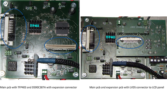
Here you can see my pcb, left pictures shows my frist pcb connector where the LVDS signals will go to my second pcb. From there (right picture) the signal will follow from LVDS connector 2 to lcd panel via cable (length about 20 cm).

Has anybody perhaps some suggestions for improving my signal? I looked for some LVDS repeater/buffer and I found DS25BR100 and DS25BR440. Could they help me to reach my goal?

I'd appreciated if somebody could help me.

Best regards

Jürgen

  • Has nobody an idea? I am now redesigning my pcb, so if I get some references then they can flow in my new design.

    Best regards,

    Jürgen

  • Hi Jurgen,

    Where is the probe point of the LVDS signals? You cannot directly probe the LVDS outputs of DS90C387A or in the middle of the bus due to impedance discontinuity. For proper differential probing, measurements should be made at the end of the 100ohm termination resistor (i.e. at receiver inputs). Have you also performed a TDR measurement on the differentials lines between the two pcb boards?

    Dac Tran

    SVA / APPS

  • Hi Dac,

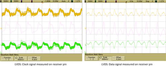
    thanks for your fast response. I measured now the signals on receiver input and it looks like this:

    Left pictures shows the lvds clock, where green and yellow are the real signal and blue the difference. Right pictures shows on lvds channel, the other channels look nearly equal. It looks like if the low state could not reached, what do you think?

    Best regards

    Juergen

  • Juergen

    I think that what Dac was asking was how you were probing the signals with the oscilloscope - ideally, you will place a differential probe across the termination resistor at the receive end of the transmission line.   Can you give us more detail on where you are placing your 'scope probe?

    Mark


  • Oh sorry for misunderstanding.

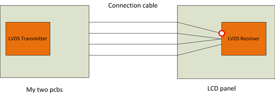
    I meausered on receiver side with two scope probes directly on the receiver pins.

    I allways measured the positve and negative from each channel and create the difference function. All systems where powered on and got some data from my graphic controller. I use an Agillent oscilloscope with a bandwidth of 500MHz. At the moment I try to find an TDR in our house, if I get one, I will do a meausrement and calculation mircostripe impedance Z0.

  • Hi Juergen,

    I would suggest measuring the LVDS signals again using a differential probe (vs single-end). Reason being the derived differential signals made using single-ended measurements may be misleading if probes are not 100% identical due to variations (ie loading, skew, etc), noise, and grounding.  In addition, since you are running the LVDS datarate at 504mbps (or 72*7), be sure the probe and scope have sufficient bandwidth.

    Dac Tran

    SVA / APPS

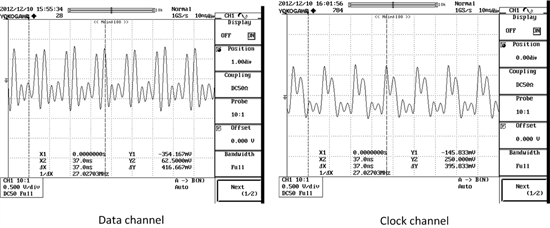
  • Finally I found a differential probe with sufficient bandwidth and measured data and clock lines. Following images shows a data and a clock channel:

    The differential probe was directly on the receiver input pins, all systems were turned on.m It looks like I have some strong refelction...

  • I analysed the above pictures and one strange thing I noticed. While the clock is HIGH it looks like that the data channel has a HIGH/LOW/HIGH state (while clock is HIGH). Could this be an power supply problem where the HIGH state collapse and generate an adittional LOW state?

  • Hi Juergen,

    The signal quality looks more like impedance mismatching. If you suspect that it may be from power supply noise related, you can probe LVDS signals and power supply together at the same time. Then observe if the supply noise follows the waveform ringing or any signature of the noise.

    Some additional questions:

    1 ) Do the differential pairs layout have controlled impedance of 100ohm differential?

    2 ) What is the impedance of the cable?

    Dac Tran

    SVA / APPS