This thread has been locked.

If you have a related question, please click the "Ask a related question" button in the top right corner. The newly created question will be automatically linked to this question.

TPS2546: TPS2546 USB certification issue

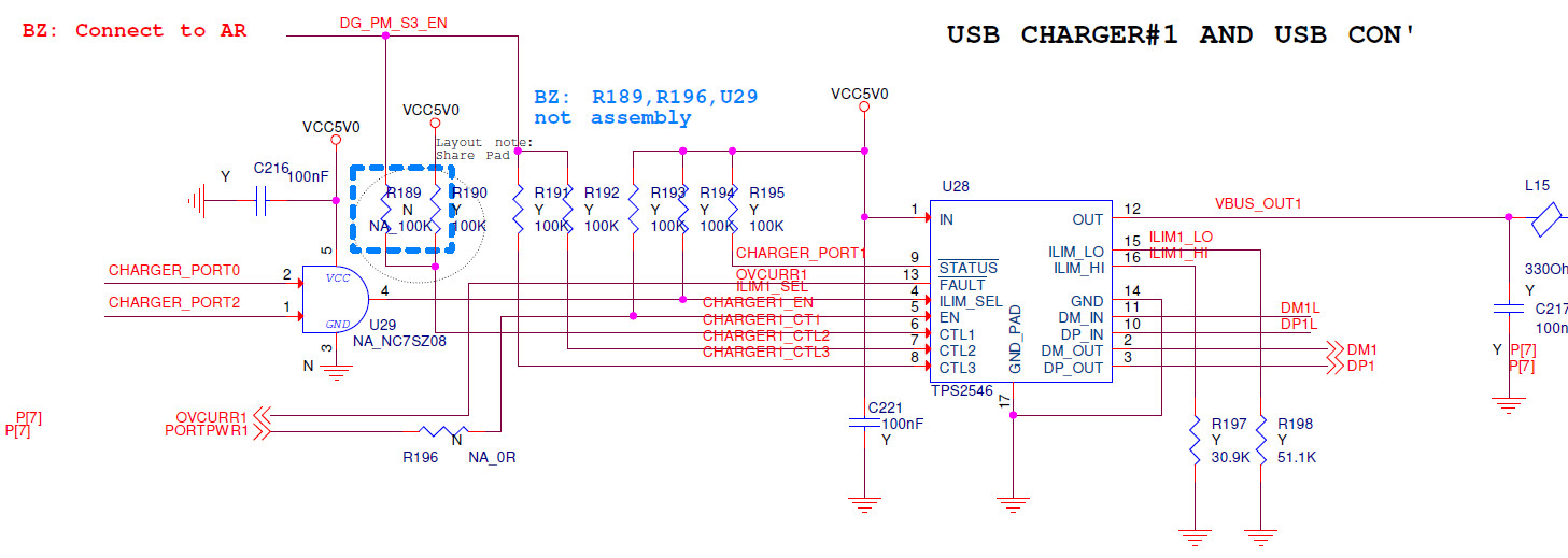
Part Number: TPS2546
Other Parts Discussed in Thread: TPS2547, , TPS2549

Hi 

My customer used  TPS2546 can not pass the USB certification. We got fail about A4.9: Host Test J/K, SE0_NAK (EL_9) in SDP / CDP mode.

SDP mode Test K in D+ is over 20mV and D- is pass. CDP mode Test J in D- is over 20mV and D+ is pass. Do you have any suggestions? Thanks for help~

  • AJ,

    Could you share the schematic for the design so that our team can review and provide you input on this certification failure?

    Regards,
    Atiq
  • Dear Atiq.

    Please reference on below and thanks for kindly help~

  • Dear Atiq.

    Update more. Thanks~

  • has the voltage been measured on DM_OUT and DP_OUT pins when the test fails? Please also confim the mode the device is in when the test fails(CTL* mode level)
  • Dear Yoon.

    When test fail the DM_OUT is 24~27mV and DP_OUT about 400mV. Test is in CDP mode.

    We change TPS2546 to TPS2547 also got fail. Please kindly help it.~

  • Hi AJ, I think it may be the USB host/hub controller contributing to the offset. Could you check the DM_OUT and DP_OUT voltage, DM_IN and DP_IN while EN = low. This should disable the signal switch. If offset voltage measured on DM_OUT and DP_OUT while EN = low, the offset may be driven by the USB host/hub controller.
  • Dear Yoon,

    We test as below, if need any more information, please let me know, thanks! 

    While EN = low.
    DM_OUT=5.177V
    DP_OUT=4.084V
    DM_IN=27mV
    DP_IN=21mV
    While EN = low, under Test J condition.
    DM_OUT=5.177V
    DP_OUT=3.089V
    DM_IN=31mV
    DP_IN=24mV
  • Just to confirm, non driven signal lines(D+ or D-) need to be below +/-10mV to pass when measured at the connector, correct?

    What is the measurement condition?  WIth the sQuidd board attached?  Are DM_IN and DP_INs connected to the connector?  What is the connection between DP1L/DM1L and DP1L_C/DM1L_C?

    DM_OUT/DP_OUT connected to the host controller?

  • Hi,

    ‘The issue is due to a conflict between the Test_J and the BC1.2 Spec. 

    Test_J places a 400mV DC signal on the D+ line.  This happens to be within the window where the BC1.2 spec defines primary detection.

    Thus, the TPS2546 sees a primary detection voltage on D+ and since the TPS2546 is in CDP mode, it responds by putting VDM_SRC on D-. 

    In a normal CDP situation the D- voltage would be around 0.6V.  But this is not a normal situation since the D- line is loaded with two 45 ohm resistors in parallel for a total D- resistance to ground of 22.5 ohms. 

    The maximum D- load in primary detection is 250uA.  Meanwhile, 0.6V into 22.5 ohms is over 25mA. 

    So the Test_J  is both triggering primary detection and placing a short circuit on D-.  Now the TPS2546 is designed to protect against a primary detection short and has a 1mA (typ) current limit on the D- output. 

    So now we can see that a 1mA current limit into a 22.5 ohm load will obtain the 22mV voltage on D-.

    This issue only occurs when a Test J packet is sent on a CDP with a standalone battery charging device(TPS2546 in this case), not a real world condition hence does not have impact on real application.

  • Hi Yongqiang Sun,
    Thanks for your reply.
    Cause our product need to pass USB certification, please let me know how to explain Allion Lab cause they follow USB-IF's requirement, any method to pass/waive the Test_J?
  • Dear Yongqiang .
    Do you have any suggestion? We need your help. Thanks~
  • Hi,

    if passing the Test-J is mandatory, I think customer will have to change to TPS2549, TPS2549 can pass the test-J.   we have a detailed report, please send me an email and I will share the report with you.  yongqiang-sun@ti.com