This thread has been locked.

If you have a related question, please click the "Ask a related question" button in the top right corner. The newly created question will be automatically linked to this question.

TCA9406: SCL and SDA High Frequency Oscillation

Part Number: TCA9406
Other Parts Discussed in Thread: PCA9306, TCA9617A, TCA9617B

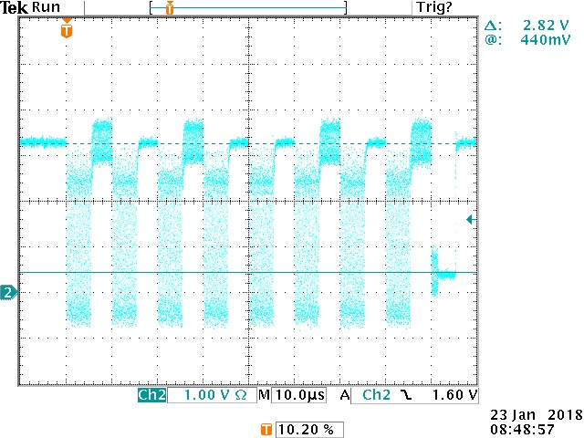
I have a board using the TCA9406 to interface between 3.3V logic external logic and 5V internal logic.   The external logic is on a motherboard and my board connects to the motherboard via a short cable.  My board generates a local +3.3V to power the "A" side of the 9406.   There is only one I2C device on my board and it is an I2C Slave.  The board works and I can cable it to a Raspberry PI, for example and everything is good.  However, when I attach it to the customers motherboard, the TCA9406 goes into oscillation.   The SDA and SCL lines will have a 20MHZ oscillation on top of the normal 100KHZ waveforms.   The customer's I2C bus is heavily loaded with lots of 5K pullup resistors and PCB traces stubs going everywhere.    

If I disconnect some of the nets on the motherboard's I2C bus, then the problem goes away.    It is not the parallel loading of the pullup resistors.   I can place 500 ohm pullups on the Raspberry PI and use a 2 meter long interface cable without causing any oscillation.  The problem appears to be the one-shots within the 9406.  These appear to getting into a mode where they keep retriggering themselves which causes this oscillation. 

Questions:

1.  Anyone have this oscillation problem before with this part?

2.  Are there any pin compatible parts that I could drop into this board?  I looked at datasheets but so far none have this pin configuration. 

Below I will paste scope shots taken on the connector of the interface cable with my board installed and then removed.   This oscillation shows up on both the "A" and "B" sides of the 9406.  I2C accesses try to work, but get numerous errors due to all the extra edges.

  • Hey Stephen,

    Can you verify a few things for me?

    1) The scope shot on the top, is this an o-scope persistence shot or is this an under sampled picture? (it's hard to connect the dots here)

    -If it is persistence, can you zoom in to cycle and take a normal scope shot. If it is under sampled, can you zoom in to one cycle and get a high sampled shot?

    2) Can we get a look at the schematics/block diagram?

    example: please include pull up resistors if possible

    -If this is something you can't share online, we can take it offline if needed.

    3) Do you know what the equivalent pull up resistance on the other board?

    4) Have you tried slowly removing pull up resistors on the other board to see if that helps?

    5) The scope shot on the bottom, are you saying this side does not see oscillation or are you saying that side is also oscillating (should be low but bounces low and high continuously)

    6) Are there any other I2C buffers in direct contact with our device?

    -I've seen instances where two buffers with offset sides connected to each other can cause oscillations such as the one in the second o-scope picture.

    7) Is picture top picture A side and bottom picture B side?

    Your Questions:

    1.  Anyone have this oscillation problem before with this part?

    This is the first time we've seen this behavior on this device.

    2.  Are there any pin compatible parts that I could drop into this board?  I looked at datasheets but so far none have this pin configuration.

    Unfortunately not, one thing you could try is using our TCA980x EVM board instead of yours and bypass the TCA9406.

    Thanks,

    -Bobby

  • Hi Bobby,

    The scope shot is undersampled.  The sweep speed is zoomed out to show several I2C clocks.   The system is in use right now, so I cannot get another scope shot until tomorrow.  I got new parts from Mouser, but they show the same symptom.   I also got samples of the TCA9617 and PCA9306.   I dead-bugged these onto perf board and wired them in to replace the TCA9406.   Those alternate devices do not oscillate.  

    The motherboard I am interfacing to is from a third party.  I do not have their schematics.  From what I can see, their I2C or SMBus is a complex nightmare.   Lots of translators, lots of slave devices, and lots of pullups.   They told me one resistor pair to remove which would isolate part of the bus.   When I did the isolation, the problem went away.   Therefore, I believe the root cause is a massive amount of noise from their motherboard.  Measuring from +3.3V on their board to SDA or SCL, I get under 500 ohms, yet their typical pullup is 5K.  

    I cannot really give my schematic, as its a actually owned by the folks hiring us.  However, the I2C interface is simple and I will try to paste in a portion of that.   The 3.3V SMBus input sees only the TCA9406.   The output of the TCA9406 goes only to a Cypress PSoC running at 5V.  

  • Below are some scope shots with the sweep speed zoomed in.   The frequency of oscillation is around 28MHZ.   I am measuring this on a connector that is on a intermediate board between the motherboard and my board with the TCA9406.   The interface from the motherboard is 3.3V level and my board is 5V level.  Therefore,  the scope shots refer to connections to the "A" side.    When the oscillations occur, it shows up on both sides,  "A" and "B" of the TCA9406.   Typically, the high level will have a ring in the waveform.  It is only the low level that will have sustained oscillations.   Once it starts oscillating on a high to low transition, the will continue for the enter interval.   It is intermittent, so some I2C transactions go through without any  oscillations.

    I added 47pF capacitors from SDA to GND and SCL to GND at the connector on the intermediate board.   This improved the performance somewhat, but did not eliminate the problem.  Probably capacitors of 100pF or greater would be required.   That is not really a fix, but a workaround.  It is only possible because they have so many parallel 5K pullup resistors.

  • Hey Stephen,

    Thanks for the additional information.

    --------------------------------------------------------------------------------------------------------------------------------------------------------------------------------------------------------------------

    "I also got samples of the TCA9617 and PCA9306.   I dead-bugged these onto perf board and wired them in to replace the TCA9406.   Those alternate devices do not oscillate."

    PCA9306 is actually not a buffer but instead a passive element device (no one shots or anything fancy). Therefore it cannot cause oscillations. The downside to this is because it does not have RTA (rise time accelerators) it does not support 1MHz I2C applications well.(Note these devices are not buffers like TCA9617)

    TCA9617A is the same in the sense there is no RTA which is also why you didn't run into this issue. (does provide buffering but generates a static voltage offset on one side of about 0.5V)

    --------------------------------------------------------------------------------------------------------------------------------------------------------------------------------------------------------------------

    "I believe the root cause is a massive amount of noise from their motherboard."

    I discussed this post with a colleague yesterday and based on the information provided, we suspect it is actually a mix of the pull up resistance and potential noise. With a low equivalent pull up resistance, the VoL when a I2C device pulls down can be large (you have more current flowing into a pull down FET whose impedance is small but constant resulting in this VoL). With a high VoL around the RTA trigger voltage you could accidentally trip the RTA if your noise pulls the bus voltage above the RTA.

    I talked to the designer of the device and he's verified the the RTAs are not edge triggered but voltage triggers and static voltage but a dynamic one (something like 50% of Vcc could be higher or lower). I've looked for some devices here and boards to see if I could do some testing to verify but it looks like I've got to order some (I don't have any at hand in the lab). This could take a day or two unfortunately.

    Based on this information I would advise to size up the pull up resistors to lower the VoL. Is this something you would be able to do if you contacted your customer about the issue?

    "I added 47pF capacitors from SDA to GND and SCL to GND at the connector on the intermediate board.This improved the performance somewhat, but did not eliminate the problem."

    This is likely helping attenuating the noise like a decoupling capacitor would but increasing the bus capacitance which has it's limits when you try to meet I2C specs (550pF max capacitance allowed for 1MHz signals)

    --------------------------------------------------------------------------------------------------------------------------------------------------------------------------------------------------------------------

    Looking at the new waveforms, it looks like those transients could damage our part because of the negative ringing which goes past the absolute max of -0.5V. Placing schottky diodes on the pins (SDA/SCL to GND) should help with limiting the negative swing and minimizing the oscillations from high to low transitions.

    Something else you could try is placing a small series resistor on the SDA/SCL lines to help limit the current and di/dt which will help reduce the inductive kickback event. Note: This can cause higher VoLs because you form a larger voltage divider so size carefully. You can refer to the link below to get a better understanding:

    ---------------------------------------------------------------------------------------------------------------------------------------------------------------------------------------------------------------

    Can I get a scope shots of both sides of the channel in one picture (side A and Side B when you pull low and it oscillates). Ideally with a low done on both sides (Picture 1 of A pulling low with both channels present and picture two of B pulling low with both channels present)

    *I am particularly interested in seeing how the logic on when RTA is triggered (digital logic wise). This may paint a better picture.

    Thanks,

    -Bobby

  • Attached is a scope shot of the "A" and "B" sides during oscillation.   As I stated previously, the motherboard that my design attaches to was designed by a third party.  They will not share the full schematic with me and they have overloaded the I2C bus in my opinion.   This third party has decided that some of their I2C devices do not need to be connected during production.  They have told me to remove two zero ohm series resistors that removed part of their internal bus.  With the bus limited, the oscillation is not been seen so far.   I will also attach a scope shot of the rising edge with the limited I2C bus and finally what it looks like with the extra I2C loads attached.

  • Hey Stephen,

    I was able to do some testing in the lab today. I set up the device at the same voltages as you used and used the internal 10k pull ups. I slowly incremented the voltage on the SCLA until I saw the signal hit the rise time accelerator. The voltage this occurred at was a little bit above 900mV. I did the same for the SCLB side with the same results. What was interesting was I was able to hold the signal at 900mV and flick the wire physically and generate enough noise to get the RTAs to trigger (I am not kidding here).

    I also changed VccA to 2.0-V and ran the same test and found the RTAs triggered at about 700mV. This tells us the RTAs trigger at about 30% of the lowest Vcc value.

    I was able to recreate the oscillations like in your situation and believe I have a better understand of the oscillation cycle.

    ---------------------------------------------------------------------------------------------------------------------------------------------------------------------------------------------

    The process in which the signal is likely oscillating:

    1) The signal is pulled low but has a large VoL (pull up equivalent resistance is too low)

    2) Either noise or inductive kickback causes the signal to oscillate and trigger the RTA

    3) RTA pulls the signal up very quickly and causes the signal to ring (inductive kickback event) for about 25nS. I believe the 25nS time could be the amount of time the RTAs stay on due to the PFET on the one shot having a turn off delay time of about 25nS.

    4) Once the RTAs turn off, but the FET on the I2C bus is still pulling low and quickly pulls the signal back down

    5) An inductive kickback event likely occurs at the bottom and oscillates there until it hits the VoL and oscillates around here for a very short amount of time. The PFET on the RTA has a small delay before turning on (physics of a FET's gate charge).

    6)  The signal rings then repeats the cycle back where RTA fully engage (likely around 10ns)

    ----------------------------------------------------------------------------------------------------------------------------------------------------------------------------------------------

    Conclusion:

    From my stand point, since you can't adjust the pull up values to lower the VoL then the only work around here is to use a device without a RTA like what you did in your previous set up. I would recommend the TCA9617B here as I am assuming you need to communicate at a 1MHz frequency.

    -Bobby