This thread has been locked.

If you have a related question, please click the "Ask a related question" button in the top right corner. The newly created question will be automatically linked to this question.

DP83867E: XI input parameters

Part Number: DP83867E

Hello, we are using DP83867ERGZT with 3.3V external oscillator connected to XI via capacitive divider as described in datasheet (Figure 28. Clock Divider).

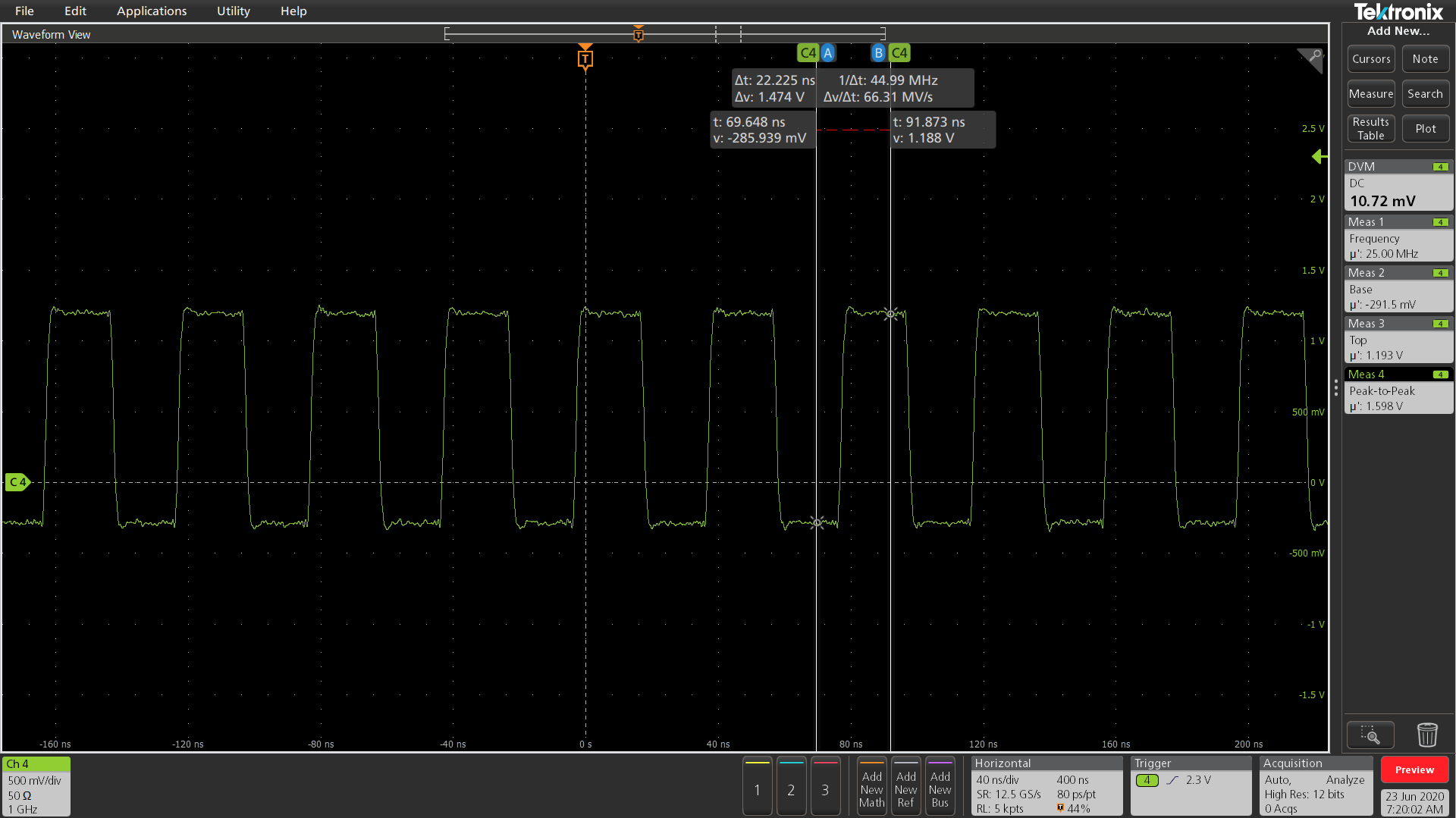
We adjusted the values of CD1/CD2 during prototype testing to meet amplitude specification defined in Electrical Characteristics.

Based on our measurements, AC coupling of signal causes opening of the protective diode of XI pin, and for that reason, base of clock signal is -380mV. It does not meet the requirements from table 7.1 Absolute Maximum Ratings where min. XI voltage is -0.3V.

The reason is clear - because of the use of a capacitive divider, the DC offset of clock signal on XI depends on the internal bias of XI (if any) and on the opening of the protection diode on XI pin. The capacitance ratio CD1/CD2 can only affect the amplitude of the signal, but does not affect the DC offset.

We think that with the use of recommended capacitive divider it is not possible to meet requirements of XI specification and absolute max. ratings.

Can you confirm to us that XI can be long time and stable operated this way (out of the requirements of absolute maximum ratings) or recommend us a better solution?

Thanks and have a nice day

JZ

  • Hi JZ,

    Can you share the CD1 and CD2 value that you used to adjust the clock pk-pk voltage?

    -Regards

    Aniruddha

  • Hi Aniruddha.

    we have two PHYs on board. Values of CD1/CD2 are: 47p/22p and 33p/15p.

    Some more information: Clock source is LVCMOS 3.3V with 50R output impedance.

    PCB traces are routed with controlled impedance 50R.

    Waveforms measured by the differential probe on CD2 are attached.

  • Hi JZ,

    For a 3.3V LVCMOS oscillator, 27pF/27pF cap divider should be sufficient. Are you seeing issues with this combination?

    -Regards

    Aniruddha

  • Hi Aniruddha,

    we started with values 22pF/22pF (because the value 22pF is already used elsewhere in design and we try to keep the number of unique values at the lowest possible level).

    Measured values for both PHY are attached - as you can see, VIH is lower than required by the datasheet ( VIH > 1.4V) and signal amplitude is 1.5Vpp which is the lowest limit required by the datasheet.

    The problem with the negative VIL level persists, regardless of the size of the capacities.

    I can replace the capacitors with 2x27p and make a new measurement, but I think the problem with the negative voltage of the VIL will remain unchanged.

    Have a nice day

    JZ

  • Hi JZ,

    Just checking, were you able to run the test with 27pF? Do they show the same voltage levels?

    Does the output voltage of the oscillator show 3.3V pk-pk signal or is it lower?

    -Regards

    Aniruddha

  • Hi Aniruddha,

    today I made the measurements just for you, with expected results.

    About oscillator - there is a LVCMOS output of clock generator:

    • Voltage level is set to 3,3 V.
    • Really measured value is 3,340 Vpp (logic signal with base near 0.0 V and amplitude 3,34 V).
    • Output impedance of clock generator driver is 50R.
    • PCB trace has controlled impedance 50R. 

    As you can see in the attached screenshot (the exact values Meas 1-4 are on the right edge):

    • Datasheet requirement for XI input voltage above -0,3V is fulfilled (Meas 2 (Base) = -291,5 mV)
    • Datasheet requirement for XI input voltage 1.5 - 1.9 Vpp is fulfilled (Meas 4 (Peak-to-Peak) = 1.598 Vpp)
    • Datasheet requirement for XI input high level >1.4 V is not met (Meas 3 (Top) = 1.193 V)
    • Datasheet requirement for XI input low level <0.45 V is fulfilled (Meas 2 (Base) = -291,5 mV)

    Thank you for your time

    Jiri

  • Hi Jiri,

    Thank you for providing more data, we are reviewing the information can comparing it with the data from when the device was tested. We will send an update by end of next week.

    -Regards

    Aniruddha

  • Hi Aniruddha,

    we are still waiting for an answer.

    Thanks

    Jiri

  • Hi Jiri,

    Apologies for the delayed reply, from the validation data this behavior wasn't observed on our test board. Would it be possible for you to send your board schematics? I can take a look to see if anything else stands out. For debug purposes, is it possible for you to supply 2.5V clock input? it would also need a capacitor divider but different values.  For 2.5V, you can use CD1=27pF and CD2=16pF as the cap divider & see if you observe the same issue. Meanwhile, I will check if we can perform some design level checks that can provide more insight.

    -Regards

    Aniruddha

  • Hi Aniruddha,

    I made two screenshots which you can see below. The first contains a clock generator used for generating 25MHz LVCMOS signal. Don't be fooled by the value of the resistors 33ohm. The total value is 50ohm (resistor 33ohm plus the internal impedance of the output buffer 17ohm). The second screenshot contains the clock input of the DP83867E PHY.

    About the proposed measurement - we can easily change the divider, as we have done many times. In the case of a changing the input clock, the situation is a bit more complicated. If we want to provide a 2.5V clock from a clock generator to PHY, we need to do two modifications. The first is to modify the board so that pin 18 is powered by 2.5V. We have checked whether it is possible and we can say that it is not simple, but it can be realized on current prototype boards.The second modification is change of the clock generator settings using I2C, because it contains specific settings for different voltages. This is relatively easy to implement. BUT for normal production, this configuration is unusable for us. I'll try to explain why - The clock generator has a limited number of OTP setting sets, and we have them all used. In addition, some settings are shared for multiple types of cards. Therefore, we cannot create unique settings for the card with the DP83867E.

    Alternatively, we can perform measurements with PHY CLK from the signal generator. But the question what this measurement should prove remains. And do you want to do this measurement if the 2.5V configuration is not usable in serial production?

    Have a nice day

    Jiri

    CLOCK GENERATOR:


    PHY CLK INPUT:

  • Hi Jiri,

    Thanks for the additional information. Would it be possible for you to send over rest of the PHY schematics? If you have confidentiality concerns you can send it over offline via your local TI TSR/FAE.

    Regarding my experiment, I wanted to check if the behavior changes based on the voltage. If it is easier to provide a 2.5V clock via signal generator then that should also be ok. Adding to my previous request, would you also be able to measure the DC voltage on the XI pad with capacitive divider (without the oscillator driving) ?

    -Regards

    Aniruddha