This thread has been locked.

If you have a related question, please click the "Ask a related question" button in the top right corner. The newly created question will be automatically linked to this question.

[FAQ] DS90LV011A: LVDS Driver to Sub-LVDS (S-LVDS) Receiver

Part Number: DS90LV011A

How do I interface between a Sub-LVDS receiver with an LVDS driver?

  • In order to use an LVDS driver such as the TI DS90LV011A and pair it with a Sub-LVDS receiver, a step-down resistor network must be used in order to provide the proper interface between the LVDS driver and Sub-LVDS receiver. The figure below displays the differences between an LVDS and Sub-LVDS driver outputs. Since an LVDS driver has a typical fixed common mode voltage output of 1.2V and typical differential voltage swing of 350mV, the goal of the step-down resistor network is to achieve a typical fixed common mode voltage of 0.9V as well as typical output differential voltage swing of 150mV. In the table below we can see the differences between LVDS driver output levels and Sub-LVDS receiver input levels.

    Simulation Setup

    There are two methods in which you could implement this step-down resistor network. The method chosen depends on whether or not your receiver has internal termination integrated into it or not. The first section will focus on the formulas and simulations in a device without internal termination, while the second portion will focus on a device that includes internal termination.

    The simulations will be done using Keysight ADS with the TI DS90LV011A IBIS model (ds90lv001atmf.ibs) which can be downloaded on the TI website using the link: https://www.ti.com/lit/zip/snlm047

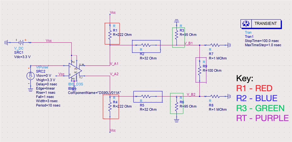
    • R1, R2, & R3 make up the resistor network that needs to be created to interface between LVDS and Sub-LVDS. Each differential pair will be made up of these three resistors.
    • R_T is the value of the termination resistor for devices that contain internal termination (100Ω will be used for this simulation).
    • R_E is the equivalent resistance of all the resistors in the resistor network.
      • Note: the Thevenin resistance of these resistors must be approximately 50Ω if the device does or does not contain internal termination; this ensures that the circuit will have a 100Ω equivalent termination resistance between the transmitter and receiver for both differential pairs. The appropriate formulas for each scenario can be seen in the sections below.
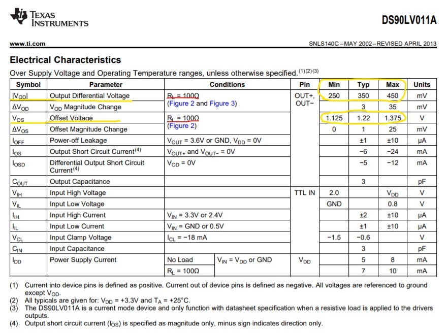
    • V_A is equivalent to the fixed common mode voltage (V_CMF) of the LVDS driver output (1.2V will be used for this simulation).
    • V_OD is the output differential voltage from the LVDS driver.
      • The values used can be obtained from the “Electrical Characteristics” section of the data sheet for your device. As seen in the datasheet below for the DS90LV011A.

    • V_B is equivalent to the fixed common mode voltage (V_CMF) of typical Sub-LVDS driver outputs (0.9V will be used for this simulation).
    • V_ID is the output differential voltage of a Sub-LVDS driver. The goal of the simulation is to obtain a value in the operating range for Sub-LVDS transmitters.
      • The values for a Sub-LVDS driver and receiver can be seen in the table below.


    Devices without Termination Resistors

    1.First verify with your datasheet if the receiver that you are using for your design contains an internal termination resistor. The formulas used are similar to obtain values with small differences taking the termination resistor into consideration.

    2.If your device does not contain internal termination then the following equations will be used:

    3.For the simulation the following values will be used:

    • V_CC = 3.3V
    • V_A = 1.2V, LVDS driver output fixed common mode voltage
    • V_B = 0.9V, Sub-LVDS driver output fixed common mode voltage
    • R_E = 50Ω 

    4.Using the formulas a, b, and c from section 2, create a system of equations in order to solve for the resistance values that will best fit the desired parameters for Sub-LVDS. The following values were obtained from the system of equations:

    • R1 = 110Ω
    • R2 = 35Ω
    • R3 = 50Ω

    Now proceed to simulate the circuit in order to verify the correct behavior.

     (Note resistors R7 and R8 are used to imitate the high impedance inputs of a receiver)

     5.The simulation shown in the figure below demonstrates a voltage swing of approximately

    • V_ID ≈ 185 mV
    • V_OD ≈ 320 mV

    V_ID falls within the desired range. If the formulas are used to obtain values for V_ID, V_CMF, & R_E with the resistor values and the measured values for V_OD & V_A then we obtain the following results:

    • V_ID = 188 mV
    • V_B = 0.85V
    • R_E = 48Ω   

    Devices with Termination Resistors

    1.The following is for the scenario in which the device that is being used for the receiver already contains a termination resistor. The process and the equations are roughly the same with just a few adjustments due to the added resistance. Firstly, ensure that the receiver being used does contain a termination resistor and obtain the value of the resistance from the datasheet.

    2.If your device does contain internal termination then the following equations will be used:


    3.For the simulation the values will be used:

    • V_CC = 3.3V
    • V_A = 1.2V, LVDS driver output fixed common mode voltage
    • V_B = 0.9V, Sub-LVDS driver output fixed common mode voltage
    • R_E = 50Ω
    • R_T = 100Ω, value of termination resistor inside device

    4.Using the formulas a, b, and c from section 2 create a system of equations in order to solve for the resistance values that will best fit the desired parameters for Sub-LVDS. The following values were obtained from the system of equations:

    • R1 = 222Ω
    • R2 = 32Ω
    • R3 = 95Ω

    Now proceed to simulate the circuit in order to verify the correct behavior.


     (Note resistors R7 and R8 are used to imitate the high impedance inputs of a receiver)

     5.The simulation shown in the figure below demonstrates a voltage swing of approximately

    • V_ID ≈ 160 mV
    • V_OD ≈ 325 mV

    V_ID falls within the desired range. If the formulas are used to obtain values for V_ID, V_CMF, & R_E with the resistor values and the measured values for V_OD & V_A then we obtain the following results:

    • V_ID = 163 mV
    • V_B = 0.9V
    • R_E = 50Ω