Other Parts Discussed in Thread: TCA6424A, TCA6416A, PCF8574A, SN74AUP3G34
I'm wondering if it's "legal" to use multiple different pull-up voltages on the output of the TCA6408A I/O expander. This seems to be the same as the question TCA6408A-Q1: Pullups vs VDDP voltages, but that question wasn't answered and seems to have been abandoned.
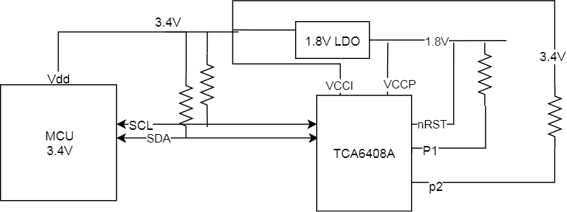
In particular, please see the attached diagram. My MCU is operating at 3.4V, and I need outputs at both 3.4 and 1.8 V logic levels. My board-space is very tight, so I'm hoping to be able to use a single I/O expander IC, instead of multiple packages. I'm using the lower voltage (1.8V) for VCCP so that there is less shoot-through current on the port's input buffer.
1) Is my diagram correct (ignoring decoupling caps), and will let me minimize power consumption?
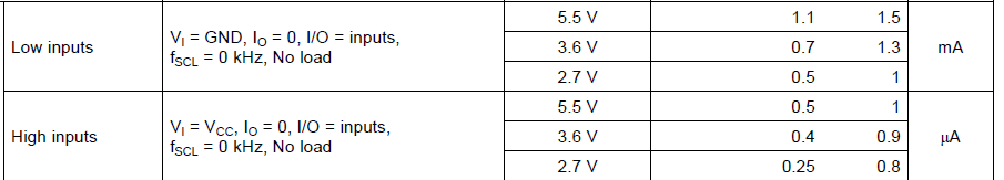
2) Is there a power consumption difference in outputting LOW on unused ports, versus leaving them as an input and connecting them to GND?
3) I don't plan to need to reset the IC from the micro, we should be able to power cycle the board if needed (though this is difficult, as it'll be welded into is enclosure), so I want to tie reset directly to a power supply rail. Since the 1.8 V rail is established second, I assume reset should be tied to it? (The datasheet figure 21 shows it using VCCP as a threshold, but figure 38 shows it's a constant threshold voltage? Table 10 has a typo saying "fising" instead of "rising"). This is similar to RESET – VCCP connection?
4) Does connecting reset directly to a rail instead of through a pull-up resistor increase the current consumption?
(And to make searching easier, I'll include the keywords TCA6416A and TCA6424A since the answers should be the same.)