This thread has been locked.

If you have a related question, please click the "Ask a related question" button in the top right corner. The newly created question will be automatically linked to this question.

DS90CR286A deserial problem

Other Parts Discussed in Thread: DS90CR285, DS90CR286A, DS90CR286

Hi, I have a board with TW8816 as LCD controller and DS90CR285 as transmitter, it's for an old car LCD display and works fine whatever the input of TW8816 is RGB888 or CVBS.

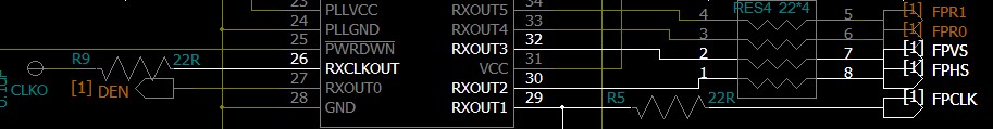
Recently, i made a deserializer board using DS90CR286A,and these two board were connected using board-to-board connector. When the input to TW8816 is RGB888,the singal deserialed good,but when the input is CVBS,then the deserialed signal is very bad. In both case, I measured the FPCLK singal at pin RXOUT1 which was deserialed from RXIN0+/- pair.The frequency of FPCLK in both cases were almost the same about 11MHz.

And the RXCLKOUT was good in both case. Because the original board can light the car LCD dislay all right, i have no reason to be suspicious about it. I can't fingure out why there is such difference in these two cases? Any advice or how should i to find out where may  problem be?

Blow is the screeshot of the FPCLK wave and the LVDS signal PCB layout.

  • Greetings,

    Looking at the scope shots, it seems the transmit clock is running at about 11MHz. These devices are rated at minimum 20MHz clock rate(please note TCIP min 15ns and max 50ns). So the device/PLL  is not intended to be used at this low frequency. Perhaps, if possible, please increase the transmit clock to at least 20MHz.

    Regards,,nasser

  • Hi, FPCLK is not the transmit clock, it is input at the pin TXIN1 of DS90CR285, and output at the pin RXOUT1 of DS90CR286. The transmit clock is 33MHz whatever the input of TW8816 is RGB888 or CVBS and it can be deserialized fine. Below is part of scheme screenshot:

    So there is something else wrong, please help me.

  • I've tried to increase the frequency of transmit clock to 48MHz or decrease to 24MHz, but no improvement and even the original signal deserialed right in 33MHz transmit clock became bad in these two transmit clock. Any more advise?

    Would it be the pcb layout problem though this circuit works in some case?

  • Greetings,

    It could be very weel related to the pcb layout but i think we should look closely before we jump to this conclusion.

    We see two issues with the scope shots you sent us:

    1). RGB888: The deserializer output clock has two humps and is not the squarewave or the smooth clock we expect. Do you have a short gnd lead on your scope probe and could this be due to the scope probing vs the actual waveform behavior? Can we shorten the scope GND lead, if indeed this is the case, and try to measure again so we can see a nice smooth clock. Or perhaps this is what it is?

    2). CVBS FPCLK: This looks like the scope is under sampled and does not look like what we have seen before. It seems to have the two humps like RGB but it is heavily distorted.

    I think to debug this, we need to divide and conquare. First we need to make sure the clock on the output of the transmiter(i.e DS90CR285) is nice and clean. Once we confirm this is the case, we should check clock on the input of the DS90CR286. This is LVDS differential pair so you should have 100 Ohm differential impedance termination. Then finally we can look at the clock at the output of the DS90CR286A. I think somewhere along the way we should be able to see at what point the clock got distorted.

    Regards,,nasser

  • Hi,

    When RGB888 as input, the FPCLK  wave deserialized from 286A RXOUT1 pin will become smooth if i make the gnd lead of the scope probe short. The scope shot as below:

    below is the scope shot of  transmit clock deserialized from 286A RXCLOCKOUT pin, which is always good whether it is RGB888 or CVBS input of video processor.

    Below is the DS90CR286 part scheme, there are 100 Ohm termination.

    And it seems that though the transmit clock could be deserialized fine from RXCLKIN pair, other signals were not the same result. I used to think that there were 7  signals mixed in RXIN0/1/2/3 pair, but there was only clock signal in RXCLKIN pair, would it the be the reason?

  • add scheme screenshot which is not inserted by CTRL+V past mode

  • Greetings,

    I believe your understanding is correct in that there are seven signals mixed in each LVDS pair(i.e RXIN0/1/2/3) and RXCLKIN pair just carries the clock signal.

    Based on looking at your schematics and earlier posts, we think the problem could be due to the fact your CVBS 11MHz signals may not be synchronous to the serializer transmit clock. On the other hand, RGB is parallel and these are synchronized. I believe to completely get rid of this problem you may need to use some logic to synchronize your 11MHz FPLK and the serializer transmit clock. I am thinking out loud here but this logic could be like  a FIFO where you are inputting the 11MHz signal and on the output you would be shifting out, in the middle of the 11MHz clock bit, by using the serializer transmit clock. Hope this is clear.

    Regards,,nasser


    And it seems that though the transmit clock could be deserialized fine from RXCLKIN pair, other signals were not the same result. I used to think that there were 7  signals mixed in RXIN0/1/2/3 pair, but there was only clock signal in RXCLKIN pair, would it the be the reason?

  • Hi, nasser,

    Thanks for your reply. I tested the car LCD pannel which was working when connecting with the DS90CR285 board, the wave of the FPCLK deserialized from DS90CR286 in panel board was almost the same as the board i made,there was the same distortion,  but the LCD pannel worked fine.it was amazing.

    In fact, i didn't connect the DS90CR286 output to the pannel directly but there was DS90CR241/124 pair between them, so it seemed that the DS90CR241 did not work in such a bad clock, but the panel worked. I dare not to believe the panel could work, but it was the truth.