This thread has been locked.

If you have a related question, please click the "Ask a related question" button in the top right corner. The newly created question will be automatically linked to this question.

ISOW1412: Only 0.6v on Visoout instead of expected 5v

Part Number: ISOW1412

Hi there,

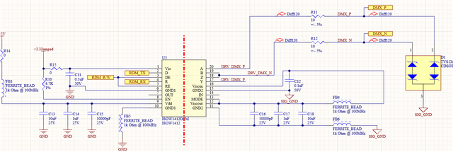
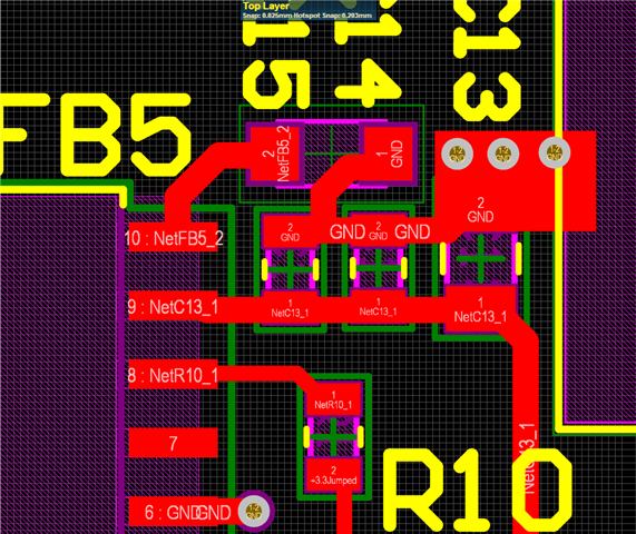
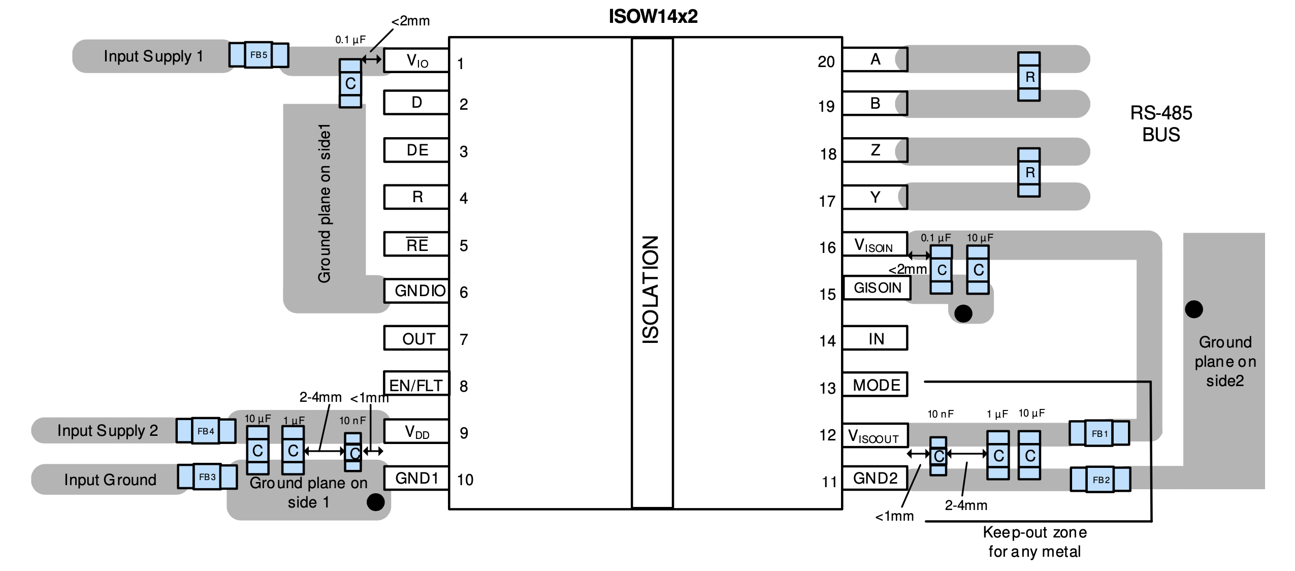
I've just build my first prototype with the ISOW1412 and I cannot make it work since I have only 0.6V on the isolated voltage output (VISOOUT)

What could cause this ? In another post you talked about Visoin connected directly to Visoout or with a ferrite bead. In my case I have a ferrite bead, should I remove it ? Here is the Schematic

Thanks

  • Hi William,

    Thanks for reaching out and sorry to hear about the issue.

    I see that EN pin is pulled-up to 3.3V VIO through a resistor. The EN pin enables / disables DC/DC converter and hence is referred to DC/DC converter GND pin 10. Its logic thresholds are also in reference to VDD supply voltage (pin 9). Since VDD is 5V while EN is connected 3.3V, the EN pin isn't really seeing a HIGH input and hence, maybe the DC/DC converter is disabled.

    For testing purpose, please unpopulate pull-up resistor R10 to float the EN pin. This should enable the DC/DC converter and you should see 5V at VISOOUT. Alternatively, please connect EN pin to VDD and monitor the VISOOUT.

    Please do the above steps and let us know your observations, thanks.


    Regards,
    Koteshwar Rao

  • Thanks for fast response !

    I tried removing the ferrite bead between Visoin and Visoout (FB4 in my schematic). -> No effect

    After that, I removed R10 (pull up on EN) and put a small wire there to enable and disable the DC/DC converter. When EN is left floating, I still have only 0.647V on Visoout. When I tie it to GND, Dc/Dc turns off and Visoout is at 0V.

    R10 (pull up on EN) was put there because in the Errata document published setpember 1st 2020 it was said that EN was pulled down inside the chip instead of pulled up...seems that this was solved !

  • Seems like I have marked this as solved, but it is not !

    sorry

  • Hi William,

    Thanks for your quick inputs.

    Did you also happen to try connecting EN to VDD (pin 9)? If not, please do try this. If it still doesn't work, then I recommend to try this with a new ISOW1412 sample to rule out any accidental damages to the IC in testing now.

    Please do test and let us know your observations, thanks.


    Regards,
    Koteshwar Rao

  • I've tried 2 boards already with exactly the same behavior.

    Connecting EN to VDD does not solve the issue

  • Hi William,

    Thanks for the confirmation.
    To debug the issue, here are some of the individual experiments that can be tried out.

    1. With EN connected to VDD, short FB5 and test. Monitor VISOOUT.
    2. Use the same 5V power supply for both VDD and VIO and test. Monitor VISOOUT.
    3. If VDD supply is current limited to a very small value, the output voltage can droop. Please confirm the current capability or limit of 5V supply. Please also confirm what is the total load current consumed by other components connected to 5V.
    4. To rule out device damage, you could measure the resistance between VDD/GND, VIO/GND, VISOOUT/GND and VISOIN/GND. Please use the respective GNDs for this measurement. This measurement is best done when the IC is depopulated.

    Please do help conduct the above experiments and share us with the observations to be able to debug the issue. Thanks.


    Regards,
    Koteshwar Rao

  • Hi William,

    Could you please confirm if you were able to conduct the experiments specified in my previous post? I believe these experiments should help us debug the issue and identify the cause. Let me know, thanks.


    Regards,
    Koteshwar Rao

  • First thing I will do this morning! Yesterday was "Canada day" so I was out. I'll keep you posted. You have been help !

  • I did the first Test (remove FB5) and it worked !

    But connecting EN to Vdd was messing with my 3.3V (Vio) and bringing it to around 4v.

    So removing FB5 (replacing it with a 0 ohm resistor), and leaving EN floating seems to be the solution for me.

    This FB5 was added after a review of my schematic with T.I. ! Maybe this also has something to do with my layout. The gnd "attach" point is far away from the chip GND1 pin, so this trace is probably already a bit inductive even without the ferrite bead (FB5) (see picture).

    Again thanks a lot! This forum works great!

  • Hi William,

    Thanks for quick test and feedback.

    I see that FB5 is added between device GND1 (pin 10) and decoupling caps, I missed to notice that earlier. The decoupling caps have to be directly connected to device supply pins and there shouldn't be anything between them. This is very critical to meet the transient currents needed by various blocks inside device. Having FB5 seems to have created an issues and replacing FB5 with a 0Ω has resolved the issue. I would recommend moving FB5 to after the decoupling caps as shown in the datasheet example (also copied below).

    I also confirmed about the power supply that EN pin is referred to, EN is actually referenced to VIO pin. I had mentioned this the opposite earlier, apologies for that. Since VIO is 3.3V and VDD is 5V, connected EN to VDD had caused an issue and hence, you were seeing 4V.

    So the solution is to retain pull-up at EN to VIO and move FB5 as shown in datasheet layout example. I hope this addresses your issue.

    Let me know if you have any further questions, thanks.


    Regards,
    Koteshwar Rao