A related question is a question created from another question. When the related question is created, it will be automatically linked to the original question.
If you have a related question, please click the "Ask a related question" button in the top right corner. The newly created question will be automatically linked to this question.
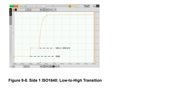
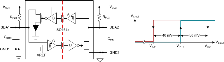
Thank you for posting to E2E! The low-to-high transition on Side 1 of the ISO164x occurs to enable bidirectional communication across a single isolator channel without its output signals being mistakenly read as input signals. Please refer to the schematic below for context:
When the SDA2 (or SCL2) input signal is LOW, the SDA1 (or SCL1) signal output will be at the VIOL1 level, mentioned in the waveform you shared and created by the diode close to buffer (B) above. However, if the input signal driven to SDA1 (or SCL1) is lower than the VILT1 threshold, the voltage level will be close to GND (0V). The slight difference in these voltage levels allows the I2C isolator to "know" when a LOW signal is being driven on side 1 of the isolator or transmitted from side 2 by comparator (C).
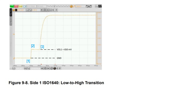
The low-to-high transition as pictured in your post occurs when SDA1 or SCL1 is driven LOW externally, and then released to the HIGH state [1]. While the device driving the LOW signal releases, the SDA1/SCL1 pin transmits a HIGH signal to SDA2 or SCL2 [2], which then returns the HIGH signal to SDA1 (or SCL1) and the pins fully release to the HIGH level [3].
More information on this design can be found in Section 8.5 of the ISO1640 datasheet and the E2E FAQ regarding our older I2C device, ISO1540, linked below:
Other Parts Discussed in Thread: ISO1541 , ISO1540 Why is the logic LOW level output voltage, V OL1 , up to 0.8V on Side1 of the ISO1540 and ISO1541 bidirectional I2C isolators?