


Other Parts Discussed in Thread: TINA-TI
Question on: ISO1212 TINA-TI Transient Reference Design (Rev. A) sllm391a.tsc
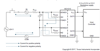
I am trying to understand better the modeling of the ISO1212 in order to verify some adjustments for my application (*) following Figure 29 found in SLLSEY7F – April 2020. My primary reason for this modeling is to 1) ensure the maximum input values are note exceeded, and 2) calculate the voltage that a bipolar-TVS diode needs to be.
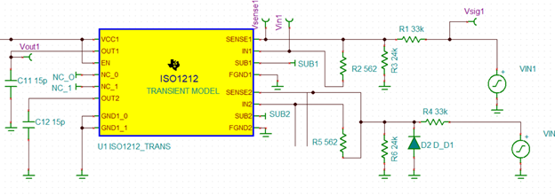
I was unable to get the above circuit to run in TINA-TI and from my search here, I read that the PSPICE model required the FGND1 and FGND2 pins to be grounded. So, I was going to model just the single channel with of AC input, and extrapolate
However, I am unable to figure out the role of D1 D_D1 and D2 D_D1 in the model. If I remove it, it appears the voltage present at the In/Sense pins exceed the maximum ratings due to an offset; even with the recommended values for Rthr/Rshunt/Rsense. However, I do not see reference to it elsewhere in any of the various application notes, etc.
Here I am modeling a 110 Vrms ( 170Vpeak ) with the recommended resistor values where I added some voltage test points. Vin1 and Vsense exceeds the -60V maximum. Is this just an artifact of the model?

Additional Question: Would the Rthr and Rshunt values remain the same when configured for a bipolar input such as in Figure 29?
(*) The system will need to detect 60 Hz AC at 120 VRMS on both polarities to achieve the required time response. Additionally, there will be several isolated/floating DC voltages which may be connected in either polarity, e.g. 0 to +125 VDC, or 0 to – 125VDC. The source of all these signals is from various relays and will be in an electrically noisy environment. The input side grounds will not be connected to the local/measurement ground. I plan on using the recommendations found in slla483.pdf, etc with respect to surge immunity, EFT, ESD as well as using some filtering.
---
Much appreciated,
Keith
