This thread has been locked.

If you have a related question, please click the "Ask a related question" button in the top right corner. The newly created question will be automatically linked to this question.

ISO1640: microprocessor location in side"2" and AD-converter location in side"1"

Part Number: ISO1640
Other Parts Discussed in Thread: ADS112C04

Hello TI's isolation parts expert team,

I am evaluating ISO1640 and ADS112C04 and try to use ADS112C04 in isolated condition by ISO1640.

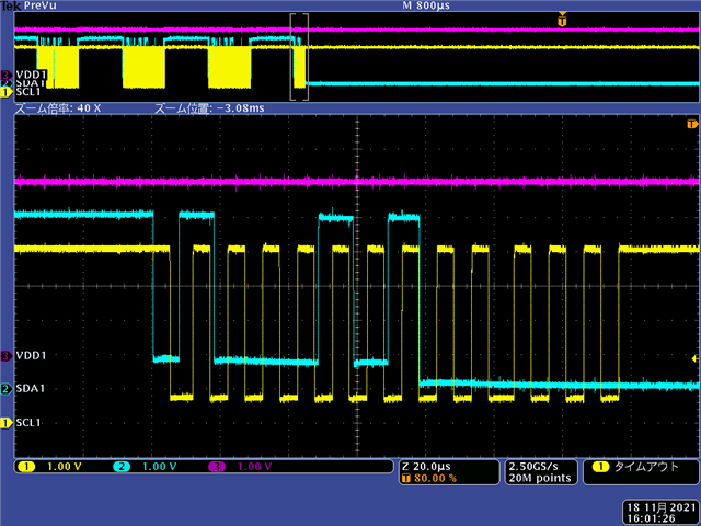
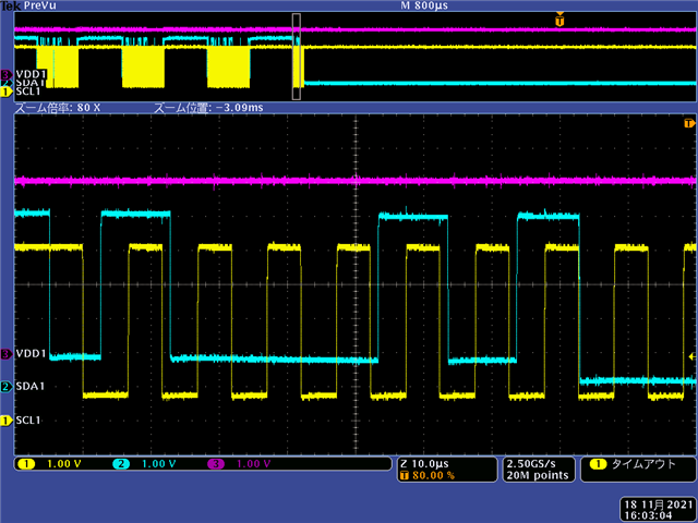
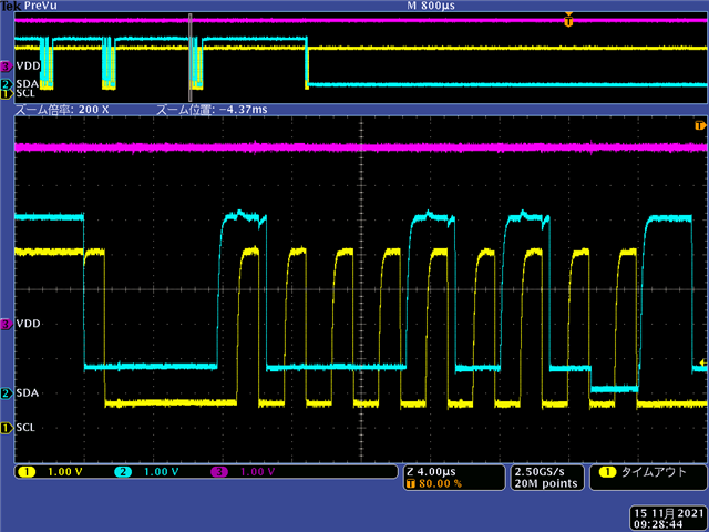
However, when I insert ISO1640 between microprocessor and ADS112C04, I2C communication fail occur suddenly and occasionally.

I discuss this phenomenon with Mr. Bob Benjamin who is expert of TI's Data Converters Forum.

Detail discussion is under way at below link(FYI);

(+) ADS112C04: SDA signal keeps Low. - Data converters forum - Data converters - TI E2E support forums

In the discussion, he reviewed ISO1640 datasheet and taught me that ISO1640 datasheet shows microprocessor is located in side1 of ISO1640 and sensor and AD converter is located in side2 of ISO1640.

However, I locate microprocessor in side"2" of ISO1640 and locate ADS112C04 in side"1".

See attachment schematic below.

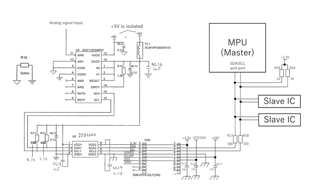
Question : Why does ISO164X series datasheet show microprocessor is located in side2 in figure9-4 and figure9-5. Is it essential for circuit design ?

Thank you very much in advance.

Best regards,

Toshihiro Sakakima

  • Hi Sakakima-san,

    Thank you for reaching out and for sharing the schematic.

    The device supports upto 80pF load capacitance on Side1 while it supports upto 400pF on Side2, this means that more devices can be connected on Side2 while not many on Side1. Since in most applications the MCU is isolated from most other I2C nodes, we connect MCU to Side1 and all other nodes to Side2 and hence the diagrams in datasheet reflect this.

    But if you have more I2C nodes on the MCU side and only one on the other device then the single device should be connected to Side1 and MCU along with other I2C nodes to be connected to Side2. I see your application has MCU and other nodes on Side2 and only one ADC on Side1, this is good.

    When there is only one node on each side, it doesn't matter which side is connected to MCU and which one is to the ADC.

    In all of the above cases, it is important to make sure that the distance between ISO1640 Side1 and the other device is kept to minimal as the logic thresholds on Side1 are sensitive and are defined differently compared to standard TTL or CMOS logic thresholds. It is also important to make sure the I/O thresholds of both ISO1640 Side1 and the other device (ADC in this case) are compatible.
    I quickly checked ADS112C04 datasheet and I see that its SDA/SCL logic specs are compatible with ISO1640 Side1, hence, I do not see any issue here.

    Could you please confirm if you tested with 1.5kΩ pull-up resistors on SDA1/SCL1 pins? If not, please try testing with 1.5kΩ and let me know. Thanks.


    Regards,
    Koteshwar Rao

  • Hi Rao-san,

    Thank you for your comments.

    I feel relieved to confirm my circuit configuration wasn't bad.

    I tested with 1.5kohm pull-up resistors on SDA1/SCL1 pin.

    And Mr. Bob Benjamin advised me to try Standard-mode(100kHz).

    So, I made 100kHz I2C firmware,and change pull-up resistor and tested.

    Unfortunately, the result is fail.

    See attachment figures for your information. 

    Expanding figure from Start condition from microprocessor to 9th bit of SCL

    Blue: SDA1

    Yellow: SCL1

    Purple : VDD1

    FYI : In schematic I attached yesterday, I replaced FL1's ferrite to 0ohm resistor Bob advised me to do so.

    If you have any comments or advises, let me know.

    Regards, 

    Toshihiro Sakakima

  • Hi Sakakima-san,

    Thanks for the update and for sharing the waveform.

    Could you please elaborate on what exactly was the failure signature?
    Did the MCU receive incorrect data from ADC? Or did you mean to refer to the SDA1 waveform having two different LOW voltages (~0.8V and ~0V)?


    Regards,
    Koteshwar Rao

  • Hi Rao-san,

    Thank you for your reply.

    The issue is ADC IC fixed SDA at low level(=0V) after 7th clock of SCL was issued and stopped communication.

    At this time, the reason isn't clear.

    Now I attached the figure when communication success (This figure shows the result operated in fast mode 400kHz).

    See below figure.

    I think you can find the difference after 7th clock of SCL.

    When communication between ADC and MCU success, we can see SDA is about 0.7V because MCU(side2) sends LOW level in SDA at 8th clock of SCL.

    At 9th clock of SCL, ADC in side1 of ISO1640 sends ACK to MCU then you can find SDA equals about 0V.

    After 9th clock of SCL, ADC release SDA line and SDA becomes high level.

    That's the correct operation.

    However, at communication fail, we can see SCL becomes LOW(=0V) after 8th clock of SCL and fixed low level(i.e., ADC IC pulls SDA line to 0V).

    That's the issue.

    If you have trouble to understand my explanation, don't hesitate to let me know.

    Thank you very much.

    Best regards,

    Toshihiro 

  • Hi Sakakima-san,

    Thank you for clarifying the failure signature and clearly explaining the exact fail condition. I understand the issue clearly now and what you are saying makes sense.

    I can also see that ADC is pulling SDA1 pin LOW at the 8th clock and after that it is held LOW by the ADC and the ADC is not releasing SDA1 pin. Thus, further communication is not happening. With that explanation, it doesn't look like the ISO1640 is causing any problem. You might have to work with the ADC team to further debug the cause for ADC holding SDA1 LOW continuously.

    If you are not convinced that ISO1640 is working fine then you can probably monitor SDA1 and SDA2 together at the same time and see if the logic levels are matching and if isolator is correctly transmitting them. This clearly confirms if ISO1640 is working fine.

    Let me know if you have any further questions, thanks.


    Regards,
    Koteshwar Rao