This thread has been locked.

If you have a related question, please click the "Ask a related question" button in the top right corner. The newly created question will be automatically linked to this question.

ISO7721: Clamping maximum current

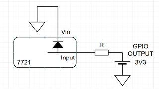
Part Number: ISO7721

At the inputs of the device, there are some diodes that clamp the signals to Vcci. 

What is the maximum permanent current allowed through those diodes?

  • Hi Ivan,

    Thanks for reaching out.

    The diodes that you are referring to at the input pins are the bypass ESD diodes. These are designed to bypass HBM ESD and protect device. Hence, they are only rated to handle transients of a few 100ns. They are not rated to clamp any continuous overvoltage applied at the pins. Hence, I do not recommend to treat these diodes as protection diode for continuous overvoltage. Instead you could add diodes externally for such protection while making sure device absolute max ratings are not violated.

    I hope this answers your question, thanks.


    Regards,
    Koteshwar Rao

  • The question I am addressing has nothing to do with an overvoltage situation. 

    In particular, the equivalent circuit is shown in the image, where Vin (power supply of the 7721) will be connected to ground. Unfortunately in this situation we cannot turn off the GPIO output that is connected to one of the inputs of the 7721. The equivalent circuit is like a 3.3V logic level permanently connected to the input of the IC and current limited by the resistor. 

    In this case, is there any information on how much would be the maximum permanent current?

  • Hi Ivan,

    Thanks for clarifying your question further, this helps.

    I understand that the input is not seeing any overvoltage condition at its pin, rather the VCC will be 0V in which case, the input pin could end up sinking in some current through the bypass diode. Please do note that your test condition is similar to the overvoltage test condition that I was referring to in my previous response. It isn't the overvoltage that is the problem, the problem is the current flowing through ESD bypass diode when voltage at input pin exceeds voltage at VCC pin by 0.5V or more. Like I mentioned earlier, the diode isn't designed to take a continuous current and it is expected to get damaged at any point of time if such a current were to be passed through it.

    Since the diode isn't designed for continuous current, we don't characterize it for continuous current either and hence, I do not have a maximum continuous current value for the diode. If you still need me to quote a current value, I would say that limiting the current to <1mA maybe okay but we will not be able to guarantee device operation as it exceeds the abs max rating of INx pin, i.e., VINx < (VCC + 0.5V) as stated in abs max ratings table in datasheet.

    I hope this helps you with what you were looking for. Thanks.


    Regards,
    Koteshwar Rao